Test report DSG-9924 · Rev C · tested November 2, 2026
Processors & AcceleratorsDevice under test
Qualcomm's HBC Silicon Hits 18x Memory Bandwidth in Lab Tests
Qualcomm's first HBC silicon shows 18x LPDDR bandwidth and 5x HBM4 energy efficiency. AI250 sampling starts in 2027, with AI300 samples in 2028.
- Read
- 4 min
- Words
- 721
- Node
- 7nm
- Operator
- Marcus Bennett
Spec summary
- HBC silicon delivers up to 18x LPDDR memory bandwidth and 5x HBM4 energy efficiency in lab validation
- AI250 inference platform sampling begins first half of 2027; Dragonfly AI300 samples in 2028
- Giaretta: energy spent moving data drops by at least one order of magnitude
- Compute die sits directly under LPDDR stack, moving data across micrometers not millimeters
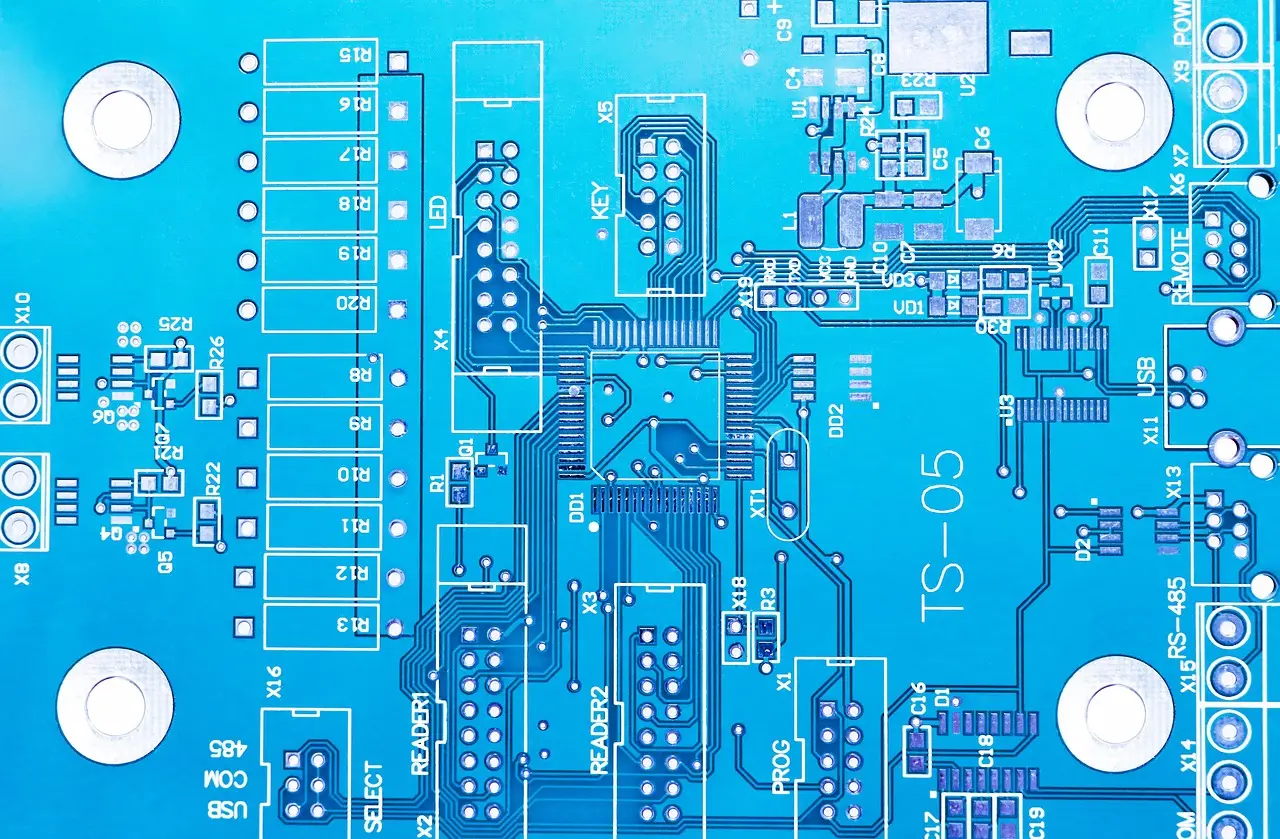
Qualcomm says its first-generation high-bandwidth computing (HBC) silicon delivers up to 18 times the memory bandwidth of LPDDR and five times the terabit-per-second-per-watt energy efficiency of HBM4. The company announced this week that the chip is in the lab, with its complete memory read-write path and near-memory computations validated at production levels using industry-standard automated test equipment.
What problem does HBC solve?
AI inference performance now depends less on raw compute speed and more on how fast a chip feeds data to its calculations. Qualcomm and others call this bottleneck the memory wall. It hits agentic AI workloads too. The wall affects both model performance and the cost of running AI workloads.
Two strategies dominate today. One keeps the model in fast on-chip memory. The other stacks high-bandwidth memory (HBM) next to the processor. Qualcomm proposes a third path: move the compute closer to the memory. It first pitched the HBC architecture in July and has repeated the argument since.
"In traditional computer architecture, you usually have DDR, you have memory of package, you have usually plenty of capacity on that, but you have a narrow link, which moves the data very slowly," said Gerardo Giaretta, vice president and general manager of datacenter CPU and AI at Qualcomm. "So far, AI has been really focusing on the HBM architecture. The challenge with that is the premium you're going to pay for HBM, a premium in terms of the cost of the solution that goes in particular on the amount of power that HBM consumes and a complex interposer and 2.5D packaging."
How does the design work?
The HBC package holds a stack of LPDDR-based memory with a compute die directly underneath it. The AI accelerator sits under the memory stack, and most workload operations run there.
"You don't have to move the data anymore in packets," Giaretta said. "You automatically have a very, very high bandwidth between the memory and the compute and you have strong energy savings simply because now you're not moving data across millimeters, but you're moving data across micrometers."
Some operations may shift to the central system-on-chip, the Dragonfly AI250, depending on implementation. The AI250 has significantly more TFLOPs than the HBC package, and the link between the two is slower. Giaretta frames HBC as a co-processor in that setup. Once instructed, the decode operations stay inside HBC, and only results travel back over the slower link — not the data itself. End-to-end performance holds up.
What does this change for the datacenter market?
Qualcomm has spent more than a year building its position as an Nvidia alternative in the AI datacenter. HBC will be integrated into the Dragonfly AI250, forming what executives call a full AI inference accelerator platform. That platform anchors the Dragonfly Rack, Qualcomm's full-stack inference infrastructure.
The roadmap runs several years:
- First-generation HBC silicon validated in the lab this week
- AI250 inference platform in production now, release due next year
- AI250 sampling in the first half of 2027
- Dragonfly C1000 CPU sampling next year
- Dragonfly AI300 samples in 2028
"You can really do inference, and it drives a clear performance advantage on the solution," Giaretta said. "AI inference is for the majority part memory bandwidth-bound. This solution gives you the bandwidth that you need at the lowest energy. From an OPEX perspective, the amount of energy you spend moving the data is at least one order of magnitude less."
He stressed that HBC is a differentiator, not just faster memory. "Our solution is putting the compute just under the memory so that you have better memory bandwidth."
Qualcomm is also working with partners on other uses for HBC beyond the AI250. The validation, Giaretta added, should erase doubts about high-yield manufacturing of the AI250 next year. "This is not a normal chip. This is the first time that somebody has done something like this. We usually don't do a blog or a pre-briefing for a bring-up of a chip. The reason why we decided to do that is exactly because it's completely new technology and it's a good validation of what we will see next year in terms of high-yield manufacturing."
via qualcomm.com (Original)
More from Marcus Bennett
Show full bio
News editor covering regulation, policy and their impact on hardware layer of artificial intelligence at Die Signal.
591 articles
Same lot · LOT-3609
- DSG-702345nmQualcomm HBC Claims 6x HBM Bandwidth Per Watt By Stacking Compute Under DRAM
- DSG-14095nmQualcomm Validates HBC Test Chip With 18× Bandwidth Claim
- DSG-874065nmQualcomm Validates HBC Stacked Memory, Targets 2027 AI250 Sampling
- DSG-68665nmQualcomm's Hexagon NPU Gains 50% More Memory Bandwidth
- DSG-712865nmQualcomm Redesigns Hexagon NPU for On-Device Agentic AI