Test report DSG-7023 · Rev D · tested October 15, 2026
Memory & StorageDevice under test
Qualcomm HBC Claims 6x HBM Bandwidth Per Watt By Stacking Compute Under DRAM
Qualcomm's HBC stacks compute dies beneath DRAM and claims 6x HBM's bandwidth per watt, targeting the AI memory wall head-on.
- Read
- 2 min
- Words
- 341
- Node
- 45nm
- Operator
- Amara Osei
Spec summary
- Qualcomm claims its HBC technology delivers 6x the bandwidth per watt of HBM.
- HBC places compute dies directly beneath the DRAM stack rather than beside it.
- The design targets the AI memory wall, the key bottleneck in accelerator performance.
- The claim was reported by Wccftech and awaits independent validation.
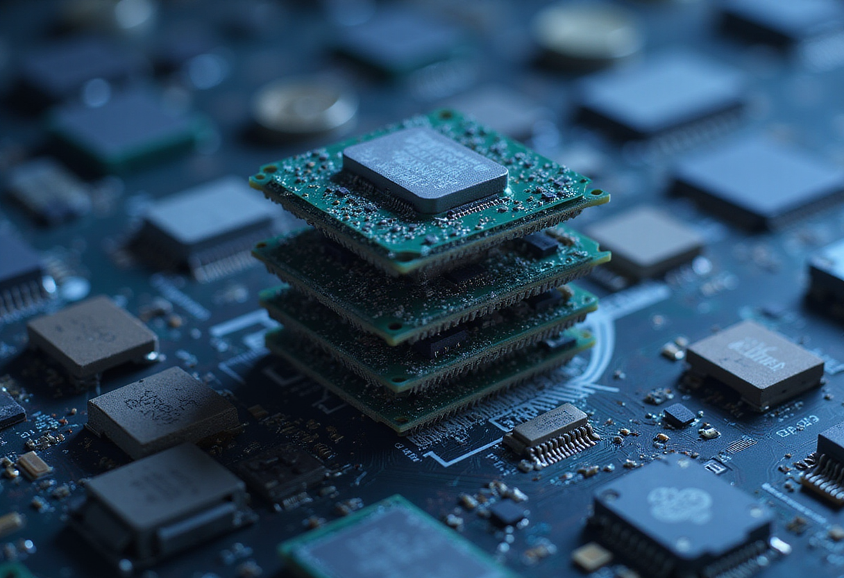
Qualcomm claims its HBC technology delivers six times the bandwidth per watt of conventional HBM, according to a report published by Wccftech. The figure targets the single largest bottleneck in AI accelerator design: memory bandwidth per watt.
The claim rests on where HBC places the processor. Instead of sitting beside DRAM packages on a substrate, compute dies sit directly beneath the DRAM stack. Shorter interconnects cut the energy cost of every byte moved between memory and logic.
What problem does HBC attack?
AI inference and training workloads are increasingly limited not by raw compute, but by the rate at which data reaches the compute units — the so-called memory wall. HBM stacks already place DRAM close to accelerators, but they remain separate packages with a defined interface cost in power and latency.
HBC collapses that distance. By integrating logic underneath the memory itself, Qualcomm aims to move data across far shorter paths at a claimed 6x improvement in bandwidth per watt over HBM.
For datacenter operators, bandwidth per watt translates directly into operating cost: every joule saved per gigabyte moved lowers the total cost of running large language models and other memory-intensive workloads.
Why does stacking order matter?
Conventional HBM places the memory stack on an interposer next to the GPU or ASIC. HBC inverts the arrangement, embedding compute beneath the DRAM layers. The physical change reduces wire length between storage and processing, which reduces signal energy and increases the feasible data rate.
The 6x bandwidth-per-watt figure is the headline specification Qualcomm puts forward against existing HBM implementations. Wccftech reports the claim as part of Qualcomm's push against the AI memory wall.
What comes next?
Qualcomm has not yet published a full product roadmap around HBC in the reported material, and independent validation of the 6x figure remains outstanding. The claim nonetheless signals where the next competitive front in AI silicon lies: not more FLOPS, but more bytes per watt.
Six times the bandwidth per watt, if it holds, would reset the efficiency baseline for AI memory.
via Google News: HBM memory (Source)
More from Amara Osei
Show full bio
Staff writer covering money, funding and market shifts around hardware layer of artificial intelligence at Die Signal.
381 articles
Same lot · LOT-C1CB
- DSG-109114nmChinese AI Chipmakers Lift Prices as HBM Shortage Tightens Supply
- DSG-995110nmSamsung: HBM to Absorb Nearly 30% of Global DRAM Capacity Next Year
- DSG-161214nmAI Demand for HBM Pushes Ordinary RAM Prices Above Cutting-Edge Chips
- DSG-251520nmMicron: AI Compute Outruns HBM Bandwidth 3x Every Two Years
- DSG-310110nmHBM stays a hyperscaler-only memory, locked to AI accelerators