Test report DSG-8740 · Rev E · tested November 2, 2026
Memory & StorageDevice under test
Qualcomm Validates HBC Stacked Memory, Targets 2027 AI250 Sampling
Qualcomm's two-layer HBC test stack beat HBM4 by 5x on bandwidth-per-watt, short of its 6x target. Dragonfly AI250 sampling starts H1 next year.
- Read
- 4 min
- Words
- 796
- Node
- 65nm
- Operator
- Priya Raman
Spec summary
- HBC validation measured more than 5x HBM4 energy efficiency on bandwidth-per-watt, against a 6x projection.
- Measured bandwidth was categorized at 18x external LPDDR5X; no absolute figures disclosed.
- Test stack had 2 DRAM layers; shipping products will have 4.
- Dragonfly AI250 begins sampling in H1 of next year; no launch date set.
- HBC capacity is projected to exceed current HBM4 implementations.
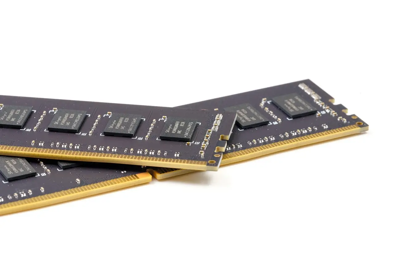
Qualcomm has measured its High Bandwidth Compute (HBC) stacked memory at more than five times the energy efficiency of HBM4, on a bandwidth-per-watt basis, in initial validation tests conducted at its San Diego labs. The figure falls short of the company's own six-fold projection, but Qualcomm says the result is sufficient to move the architecture toward mass production and commercial sampling next year with its Dragonfly AI250 data center accelerator.
The validation, announced this morning, marks the first public proof that HBC works at all. Qualcomm also categorized measured memory bandwidth at 18 times higher than external LPDDR5X, though it did not disclose specific bandwidth figures. Those two claims anchor the announcement. Both come from the company's own testing of an early sample, not from independent verification.
What is HBC and how does it differ from HBM?
Qualcomm first announced HBC at its 2026 Investor Day. The architecture places multiple layers of DRAM on top of a small compute die, rather than stacking DRAM on a passive base die connected to a host processor over an ultra-wide memory bus, as High Bandwidth Memory (HBM) does.
The compute die at the bottom of the stack is not a full processor. Qualcomm's design runs the most memory bandwidth-intensive operations on that die and sends the results back to the larger compute die at the center of the processor. The stated goal is to place memory and compute as close together as feasible.
The core argument is arithmetic about distance. Moving data costs energy, and moving large amounts of data over long distances costs more. Placing memory directly on a compute die eliminates even the short hop of an HBM connection, never mind the far longer path to off-package LPDDR5X. The savings, Qualcomm argues, can be reinvested in chip performance or in clustering more chips within the same energy footprint.
Does HBC cut manufacturing costs?
Qualcomm claims it does, with a specific structural change. HBM's wide memory bus requires advanced packaging such as CoWoS (Chip-on-Wafer-on-Substrate, TSMC's 3D stacking process) or EMIB (Embedded Multi-die Interconnect Bridge, Intel's silicon-bridge packaging) to connect HBM stacks to a compute die and memory controllers.
HBC shifts most computation to the die under the memory. Far less bandwidth is then needed to link that die to the larger processor die elsewhere on the package. That connection can use cheaper traditional 2D organic substrates instead of advanced packaging.
The complexity is reduced, not eliminated. HBC still requires bonding multiple DRAM dies — wafers, in Qualcomm's case — on top of another die using TSVs (through-silicon vias, vertical electrical connections through a chip). The company has narrowed the difficult manufacturing steps from memory stacking plus die-to-die connectivity down to memory stacking alone.
On capacity, the design uses LPDDR5X DRAM dies rather than the thin, high-performance dies HBM requires. Qualcomm has not outlined final performance, but it projects an HBC stack's capacity will exceed what current HBM4 implementations achieve.
What did the validation actually test?
The tested hardware was modest. The early sample stack contained only two layers of DRAM dies. Shipping products will have four layers, so Qualcomm has not yet tested full-sized stacks.
Qualcomm used an automated tester to measure the stack both as an LPDDR5X device and as an HBC device. Three findings emerged:
- The two-layer stack functioned, proving the concept is manufacturable.
- Energy efficiency exceeded five times HBM4's own specifications, short of the 6x target.
- Bandwidth registered at 18x external LPDDR5X, with no absolute figures disclosed.
Qualcomm says the testing also covered thermal behavior. It offered no detail. That silence matters, because a more active compute die as the base of a stacked memory architecture is expected to generate more heat, and thermal management remains one of the major technical hurdles the company has yet to address publicly.
What comes next?
Dragonfly AI250, the successor to the Dragonfly AI200 accelerator due this year, will be the first product to integrate HBC. It has no launch date. Qualcomm says sampling begins in H1 of next year, which follows an earlier statement that sampling would start this year.
HBC is not confined to data center parts. Qualcomm has previously said it will bring the technology to consumer-focused Snapdragon products, without specifying timing or product categories.
The commercial bet is total cost of ownership. If HBC delivers, Qualcomm expects AI inference accelerators that are more energy efficient and cheaper to build than contemporary designs — cheaper to operate and, ideally, cheaper to acquire than GPUs for large inference workloads. Every promise here rests on validation hardware half the size of the shipping part, and on thermal data the company has not published.
via ServeTheHome (Source)
More from Priya Raman
Show full bio
Correspondent covering money, funding and market shifts around hardware layer of artificial intelligence at Die Signal.
573 articles
Same lot · LOT-3609
- DSG-14095nmQualcomm Validates HBC Test Chip With 18× Bandwidth Claim
- DSG-99247nmQualcomm's HBC Silicon Hits 18x Memory Bandwidth in Lab Tests
- DSG-702345nmQualcomm HBC Claims 6x HBM Bandwidth Per Watt By Stacking Compute Under DRAM
- DSG-184214nmQualcomm Validates HBC Silicon: 18x Bandwidth Claim, AI250 Samples 2027
- DSG-98875nmSamsung: HBM to Take 30% of DRAM Wafer Capacity by 2027