Test report DSG-8708 · Rev A · tested September 29, 2026
Foundries & ManufacturingDevice under test
TSMC to Expand Chiayi Site to 10 Advanced Packaging Plants
TSMC will add five advanced packaging plants in Chiayi, reaching 10 facilities. Mass production has begun at Phase I, with three Phase II plants due by 2031 amid AI demand.
- Read
- 3 min
- Words
- 586
- Node
- 5nm
- Operator
- Grace Kim
Spec summary
- TSMC plans to expand its Chiayi Science Park site to 10 advanced packaging facilities, adding five plants.
- Mass production has started at Phase I; three Phase II facilities are expected to be completed by 2031.
- TSMC raised its full-year capital spending range to US$60–64 billion; the expansion still requires government planning and environmental reviews.
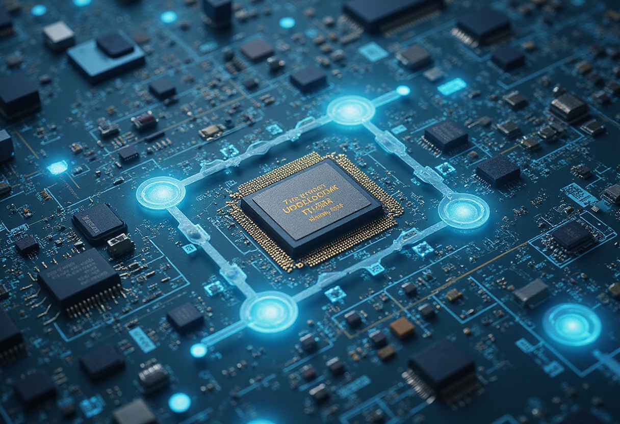
TSMC plans to add five more advanced packaging plants at Chiayi Science Park, bringing the site to 10 facilities and making it one of the world's largest concentrated locations for high-performance chip packaging. Nvidia, AMD, and Apple are among the customers driving demand for the additional assembly capacity.
Mass production has already started at Phase I of the Chiayi project, with equipment installation under way in Phase II, according to Taiwan Plus. TSMC expects to complete three Phase II packaging facilities by 2031. Planning for a later phase continues.
Packaging as a bottleneck
Advanced packaging connects multiple silicon dies, allowing processors to deliver greater speed and memory bandwidth without depending entirely on smaller manufacturing nodes. Techniques such as chip-on-wafer-on-substrate (CoWoS) integrate several components into a single tightly coordinated design.
The Semiconductor Report noted that surging AI demand has intensified pressure on advanced packaging capacity. This matters especially for data-center accelerators, which require fast memory access and high-speed communication between processing components.
Packaging has become a stubborn choke point in the supply chain. Silicon may be produced, but a finished processor still needs assembly, testing, and packaging before it can reach a server, laptop, phone, or car.
Customer impact
More capacity could smooth production schedules for Nvidia and AMD, which supply the AI and data-center markets, and for Apple, which depends on advanced semiconductor manufacturing for consumer devices. Taiwan News reported that TSMC's Chiayi plans are closely tied to advanced packaging demand.
The expansion will not remove every bottleneck. Chip design, wafer production, memory supply, and testing must all align before finished products ship. A larger packaging network may eventually support steadier deliveries of AI servers, graphics hardware, and premium electronics, but the effect will be gradual.
Concentration in Taiwan
TSMC is expanding manufacturing in the United States, Japan, and Germany, yet Taiwan remains central to its most complex packaging work. The reason is practical: packaging plants operate most efficiently close to the wafer fabs producing the underlying silicon.
The Taipei Times reported that the broader expansion spans several Taiwanese science parks. Linking Chiayi with manufacturing centres in Tainan, Kaohsiung, Pingtung, Taichung, and Hsinchu creates a dense domestic network of engineers, suppliers, and specialist equipment.
That concentration gives TSMC speed and efficiency, but it also creates exposure. Power disruptions, water shortages, transport problems, or severe weather could affect a large part of the operation at once.
Capital and competition
TSMC raised its projected full-year capital spending range to between US$60 billion and US$64 billion, according to the Taipei Times. The increase reflects the scale of demand for leading-edge manufacturing and packaging, particularly from the AI sector.
Agenzia Nova reported that the expansion still requires government review, including planning and environmental assessments, before construction contracts can advance.
The buildout places pressure on Intel and Samsung, both developing their own advanced packaging services. If TSMC secures capacity for leading chip designers first, competitors may find fewer customers willing to wait for alternative networks to mature.
Next steps
The immediate milestone is regulatory approval. Taiwan's National Science and Technology Council has opened a public consultation for the next stage, followed by feasibility work and further planning reviews.
If construction stays on schedule, the benefits should appear through more predictable chip deliveries rather than a sudden improvement. The next generation of computing will depend not only on who makes the smallest transistor, but also on who can package complex parts together quickly, reliably, and at scale.
via Google News: TSMC (Source)
More from Grace Kim
Same lot · LOT-C1BA
- DSG-87815nmTOPPAN and Broadcom open Singapore's first high-end AI-chip substrate plant
- DSG-379245nmTSMC Recasts Advanced Packaging as a Design Software Problem
- DSG-746720nmTSMC Crosses $2 Trillion Market Cap on AI Foundry Demand
- DSG-688310nmUS Pushes to Cut Taiwan Chip Reliance, but Taipei Stays Central
- DSG-35237nmTSMC Secures Approval for Sub-1.4 nm Manufacturing Plants