Test report DSG-4144 · Rev C · tested October 10, 2026
Foundries & ManufacturingDevice under test
TSMC and GlobalFoundries Tie Up $2 Billion on US Advanced Packaging
TSMC and GlobalFoundries have agreed to a $2 billion deal to expand advanced packaging capacity in the United States, addressing a documented back-end bottleneck that has constrained domestic AI chip output.
- Read
- 3 min
- Words
- 565
- Node
- 14nm
- Operator
- Grace Kim
Spec summary
- TSMC and GlobalFoundries agreed on a $2 billion transaction targeting US advanced packaging capacity, per a semivision report
- Deal addresses back-end assembly, including CoWoS, InFO, 2.5D/3D stacking and hybrid bonding capacity
- The CHIPS and Science Act authorized $52.7 billion; GlobalFoundries received $1.5B and TSMC $6.6B in publicly announced awards
- September 2024 Commerce Department strategy identified assembly and test as the lowest-capacity link in the US semiconductor value chain
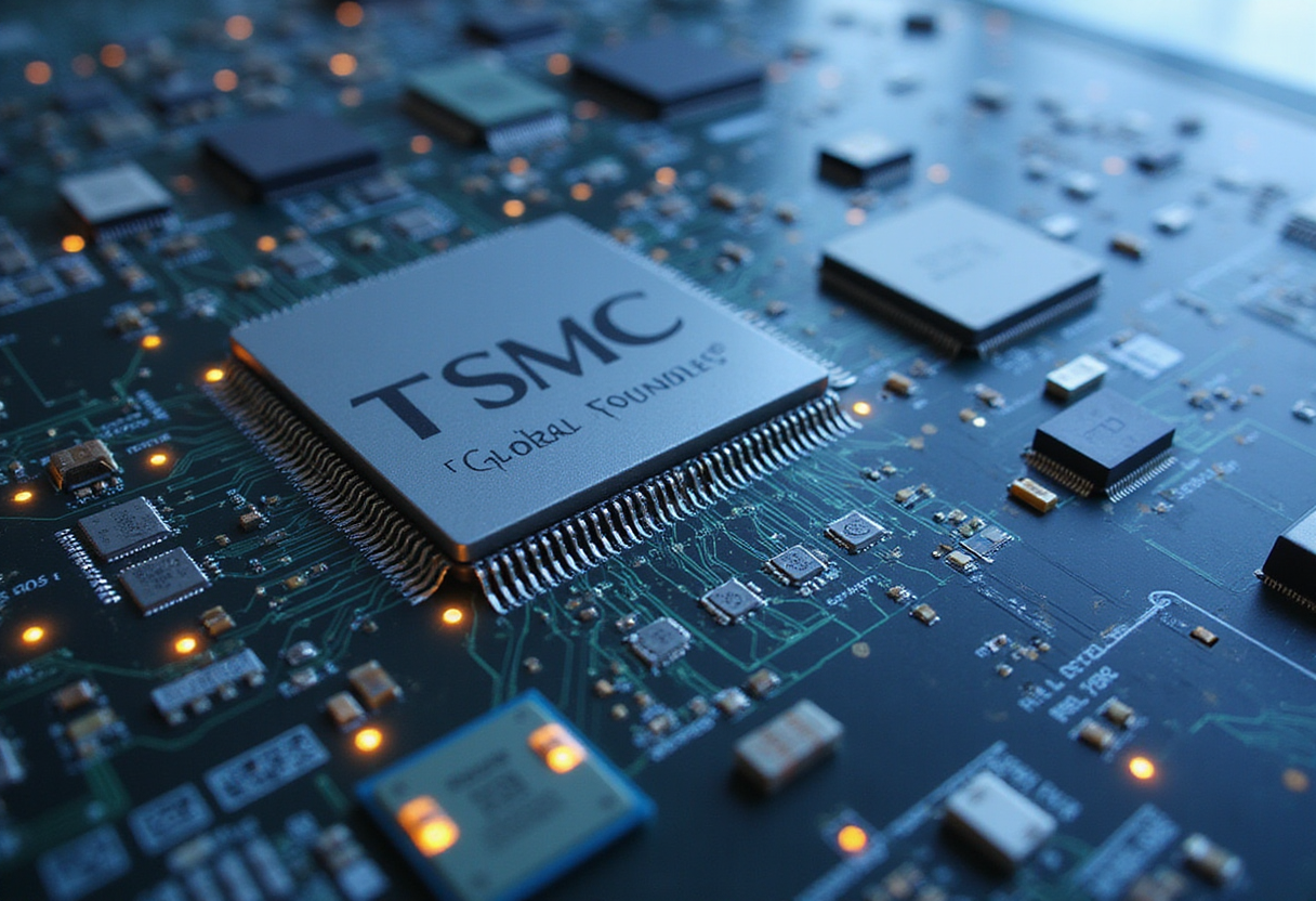
TSMC and GlobalFoundries have struck a $2 billion agreement aimed at expanding advanced packaging capacity inside the United States, according to a semivision report on the deal. The transaction places the world's largest contract chipmaker and the largest US-domiciled pure-play foundry into direct collaboration on the back-end assembly segment that has lagged domestic wafer fab construction.
What does advanced packaging actually involve?
The packaging segment covers the manufacturing steps that occur after a silicon wafer leaves the foundry floor: chiplet integration, 3D stacking, through-silicon via (TSV) interconnects, and hybrid bonding. These processes now determine throughput for AI accelerators, high-bandwidth memory stacks, and data-center processors more than transistor density alone.
- CoWoS (chip-on-wafer-on-substrate): TSMC's mainstream platform for stacking GPU, logic, and HBM dies
- InFO (integrated fan-out) wafer-level packaging: dominant in mobile and Apple silicon
- 2.5D and 3D stacking via TSVs: required for high-bandwidth memory integration
- Hybrid bonding: copper-to-copper direct interconnect at sub-micron pitch, replacing solder bumps
Demand for CoWoS specifically has run ahead of supply since 2023, with NVIDIA H100, H200, and AMD MI300 accelerator shipments repeatedly constrained by packaging throughput rather than wafer capacity.
Why does the US need this back-end capacity?
The CHIPS and Science Act of 2022 authorized $52.7 billion in semiconductor incentives. Public awards since then include TSMC ($6.6 billion for Arizona), GlobalFoundries ($1.5 billion for Malta, NY and Burlington, VT), Samsung ($6.4 billion for Taylor, TX), Intel ($8.5 billion), and Micron ($6.1 billion for Idaho and New York).
Front-end fab construction has tracked those awards. Back-end packaging has not. The Department of Commerce's National Strategy on Microelectronics, published September 2024, identified assembly and test as the lowest-capacity link in the domestic value chain relative to global benchmarks.
GlobalFoundries' existing US footprint sits within a 150-mile corridor, with TSMC's Phoenix complex and the Albany Nanotech research line both reachable within a single logistics day. Co-locating advanced packaging with wafer fabs reduces trans-Pacific shipment of partially finished silicon.
What will the $2 billion fund?
The reported transaction value would cover capital equipment, process tool installation, and qualifying test runs rather than greenfield construction, based on the typical structure of foundry-to-foundry packaging collaborations. Hybrid bonding tools alone list at $10-30 million per unit, and a single packaging line requires dozens of TSV etchers, bonders, and metrology instruments.
A line of CoWoS-class capacity typically costs $4-8 billion to qualify and ramp, suggesting the announced figure covers one partial line, multiple smaller lines, or a multi-year equipment schedule with phased payments.
What remains undisclosed?
The headline reports the deal value but does not specify:
- Whether the figure represents an equity investment, technology licensing, a multi-year supply contract, or a combination
- A closing date or milestone schedule
- Specific customer allocations
- Whether the agreement triggers Committee on Foreign Investment in the United States (CFIUS) review, given TSMC's status as a Taiwan-incorporated entity operating US-affiliated businesses
The deal's structure will determine regulatory treatment and the timeline for incremental capacity additions. TSMC's Phoenix fabs carry staggered ramp milestones running through 2028, and back-end capacity will need to align with those schedules to avoid creating a new imbalance between front-end and back-end throughput.
via Google News: Semiconductor supply chain (Source)
More from Grace Kim
Same lot · LOT-C1C6
- DSG-87085nmTSMC to Expand Chiayi Site to 10 Advanced Packaging Plants
- DSG-190445nmGlobalFoundries and TSMC Sign $2 Billion Silicon Interposer Deal
- DSG-974845nmGlobalFoundries signs $2bn, five-year deal with TSMC on advanced packaging
- DSG-63383nmGlobalFoundries and TSMC Agree to Build US Silicon Interposer Supply
- DSG-418165nmGlobalFoundries to Build TSMC CoWoS Interposers in US Under $2B Deal