Test report DSG-7353 · Rev F · tested October 10, 2026
Memory & StorageDevice under test
Samsung to allocate ~30% of DRAM capacity to HBM in 2025
Samsung plans to allocate roughly 30% of its DRAM wafer capacity to high-bandwidth memory next year, redirecting output from conventional DDR and graphics memory products, per Futu News.
- Read
- 2 min
- Words
- 409
- Node
- 14nm
- Operator
- Priya Raman
Spec summary
- Samsung plans roughly 30% of DRAM wafer capacity for HBM in 2025, per Futu News
- Conventional memory supply is set to tighten as a result of the reallocation
- The 30% figure refers to wafer capacity, not finished die output, so per-bit impact is larger
- HBM is the stacked-DRAM technology used primarily in AI accelerators
- Samsung has not disclosed which HBM generation will absorb the allocated capacity
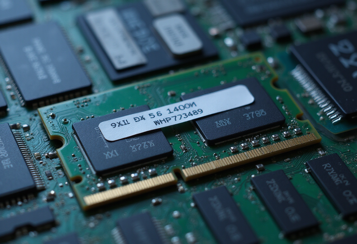
Samsung will allocate approximately 30% of its DRAM production capacity to high-bandwidth memory (HBM) next year, a reallocation that will tighten supply of conventional memory products, according to guidance reported by Futu News.
The shift pulls roughly one-third of Samsung's DRAM wafer starts out of the conventional supply pool and into stacked-DRAM production for AI accelerator customers. The 30% figure refers to wafer capacity, not finished die output; each HBM die consumes more silicon than a standard DDR die, so the per-bit supply effect will exceed the headline percentage.
What does the 30% HBM allocation mean for the memory market?
The remaining ~70% of Samsung's DRAM wafer capacity will serve standard DDR4, DDR5, LPDDR, GDDR and other conventional products. Conventional DRAM channels supply PCs, smartphones, servers, networking equipment and consumer electronics — end markets substantially larger than HBM in volume but lower margin per wafer.
A one-third reallocation of capacity toward HBM tightens the supply-demand balance for those conventional segments through 2025, Futu reported.
Why is HBM commanding a larger share of the wafer mix?
HBM is the stacked-DRAM technology used in AI accelerators from GPU and ASIC vendors. Multiple DRAM dies are vertically integrated using through-silicon-via (TSV) interconnects and connected to the host processor through a wide interface. The product sells at a substantial premium per bit compared with standard DDR5.
Samsung framed the capacity shift as a response to higher revenue potential in HBM stacks, driven by accelerator demand, the report indicated.
How does the plan compare across the industry?
Samsung is one of three principal merchant DRAM suppliers, alongside SK Hynix and Micron Technology. Industry reporting through 2024 has generally indicated that DRAM makers are expanding HBM3 and HBM3E output, in part at the expense of standard wafer starts. Futu's report focused specifically on Samsung's allocation figure and did not disclose comparable peer percentages.
What happens next?
The 2025 mix depends on HBM qualification cycles with major accelerator customers. If qualification takes longer than expected, the 30% allocation could revise downward; if demand outpaces forecasts, the share could rise. Samsung has not specified which HBM generation — HBM3, HBM3E or HBM4 — will absorb the bulk of the allocated capacity.
Conventional DRAM buyers, including PC OEMs and server integrators, will watch contract pricing in the first quarter of 2025 as the first market indicator of how the new allocation filters through to spot and contract channels.
via Google News: HBM memory (Source)
More from Priya Raman
Same lot · LOT-C1C6
- DSG-502510nmSamsung Exec: HBM to Reach Nearly 30% of Global DRAM Capacity
- DSG-828365nmSamsung: HBM to Take 30% of DRAM Wafer Capacity by 2027
- DSG-84123nmHBM Prices Set to Double as Memory Shortage Fuels Samsung Profits
- DSG-941720nmSamsung Says Memory Demand Spreads Beyond HBM; 70% of Capacity Locked in Long-Term Contracts
- DSG-440728nmSamsung Reaches 33% HBM Share, Bets on Hybrid Bonding