Test report DSG-4231 · Rev D · tested October 10, 2026
Foundries & ManufacturingDevice under test
VSMC Opens First 300mm Wafer Fab in Singapore
VSMC has officially opened its first 300mm wafer fab in Singapore, entering large-diameter semiconductor manufacturing in one of Asia's key chip hubs.
- Read
- 1 min
- Words
- 266
- Node
- 10nm
- Operator
- Elena Vasquez
Spec summary
- VSMC celebrated the grand opening of its first 300mm fab in Singapore
- The plant is the company's first 300mm-scale wafer fabrication facility
- No production capacity or process node details were disclosed in the announcement
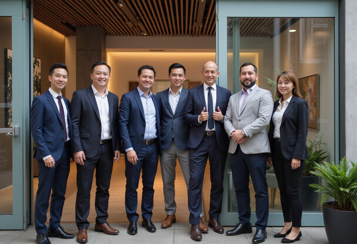
VSMC has celebrated the grand opening of its first 300mm wafer fabrication plant in Singapore, marking the company's entry into large-diameter semiconductor manufacturing.
The facility represents the first 300mm-scale operation in VSMC's manufacturing footprint. Singapore, already an established semiconductor production hub, adds another major fab to its roster of silicon wafer plants operated by global chipmakers.
The announcement came through GlobeNewswire, confirming the formal completion of the plant's opening phase.
What does a 300mm fab mean for capacity?
A 300mm — or 12-inch — wafer fab processes silicon wafers with a 300mm diameter, the industry-standard format for high-volume chip production. Compared with older 200mm lines, 300mm tools yield substantially more die per wafer, which is why the format dominates advanced logic, memory, and power semiconductor output.
For VSMC, moving into 300mm production signals a shift to larger-scale manufacturing capability. The company did not disclose output targets or process nodes in the announcement.
Why Singapore?
Singapore hosts one of Asia's densest semiconductor manufacturing clusters, spanning wafer fabrication, assembly, and test operations. The city-state supplies a significant share of global chip output and has attracted sustained investment from major semiconductor firms over decades.
Locating a 300mm fab there places VSMC inside an existing supply chain with established logistics, skilled labor, and equipment support infrastructure.
What happens next?
The grand opening marks the transition from construction and equipping to operational status. The company has not yet published details on:
- Production ramp timeline
- Target process technologies
- Customer commitments or capacity allocations
Die Signal will track further specifications as VSMC releases them.
via Google News: Semiconductor foundry (Source)
More from Elena Vasquez
Show full bio
Senior reporter covering industry trends and analytics at Die Signal.
253 articles
Same lot · LOT-C1C6
- DSG-10203nmVSMC Opens First 12-Inch Fab in Singapore, Targeting 2027 Output
- DSG-15753nmVSMC Inaugurates First 300mm Semiconductor Fab in Singapore
- DSG-296420nmVSMC Holds Grand Opening for First 300mm Singapore Fab
- DSG-90175nmVSMC Opens First 12-Inch Wafer Fab in Singapore, Targets 2027 Ramp
- DSG-289128nmUMC to Build New 22nm Wafer Fab in Singapore