Test report DSG-2964 · Rev E · tested October 10, 2026
Foundries & ManufacturingDevice under test
VSMC Holds Grand Opening for First 300mm Singapore Fab
VSMC held the grand opening of its first 300mm wafer fabrication facility in Singapore this week. The ceremony marks the joint venture's debut in 300mm wafer production and adds a new front-end node to the country's semiconductor base.
- Read
- 3 min
- Words
- 640
- Node
- 20nm
- Operator
- Elena Vasquez
Spec summary
- VSMC held the grand opening of its first 300mm wafer fab in Singapore.
- A 300mm wafer exposes roughly 2.25 times the surface area of the 200mm format.
- Greenfield 300mm projects announced across Asia over 2022-2025 have skewed toward 28nm to 90nm CMOS, analog BCD, power discretes, and mixed-signal nodes.
- Tool move-in at grand opening typically precedes first wafer-out by two to four quarters, with volume shipments following four to eight quarters later.
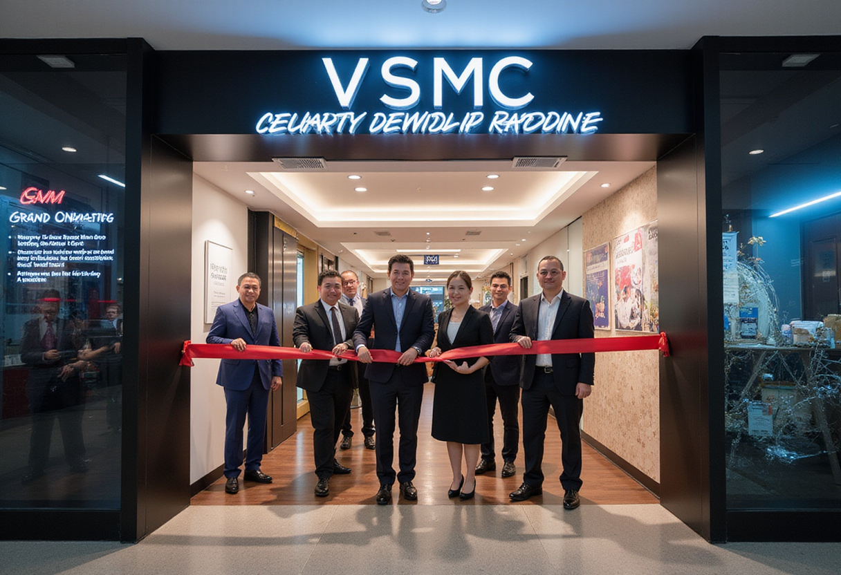
VSMC held the grand opening of its first 300mm wafer fabrication facility in Singapore, the company announced this week. The ceremony marks the joint venture's debut in 300mm wafer production and adds a front-end node to Singapore's semiconductor base.
The plant processes 300-millimeter silicon wafers — the substrate diameter that anchors advanced logic, analog, mixed-signal, and power-device manufacturing. A 300mm wafer exposes roughly 2.25 times the surface area of the 200mm format still common in specialty and mature lines, lifting die-per-wafer counts and reducing per-chip cost at high-volume utilization.
What does "first 300mm" change for the company?
The Singapore site is VSMC's inaugural 300mm fab. Until now, the joint venture's manufacturing footprint has centered on smaller wafer diameters. The 300mm designation places VSMC inside the wafer-size cohort where most greenfield capacity is now being constructed across the foundry and IDM space.
What does the announcement disclose?
The public release confirms the grand-opening event and the 300mm designation. It does not specify cleanroom size, equipment fit-out status, monthly wafer-out target, technology nodes, ramp schedule, or product mix.
Operators in this segment typically disclose these figures at groundbreaking or at formal ribbon-cutting. A fuller set of specifications is likely to appear in corporate filings or earnings disclosures.
Why does 300mm matter on the cost line?
Each process step on a 300mm wafer handles more die area than the equivalent step on 200mm. Lithography, etch, deposition, inspection, and metrology tools built for the format support higher wafer-per-hour throughput and tighter overlay control.
Once capital expenditure is amortized, the format delivers lower cost per die on mature and specialty processes — analog, mixed-signal, power management — where chip areas are larger and die-per-wafer counts scale sharply with wafer diameter.
What 300mm cohort does this fab join?
Greenfield 300mm projects announced across Asia over 2022-2025 have skewed toward mature and specialty nodes — 28nm to 90nm CMOS, analog BCD, power discretes, and mixed-signal — rather than leading-edge logic. VSMC's Singapore plant enters that cohort.
Operators in this wafer-size class cite the same cost logic: more die per run, lower per-die cost at volume, and a smaller footprint per chip on mature process flows. Singapore has hosted 200mm fabs from global operators for two decades; the addition of a 300mm site marks a generational expansion of the country's front-end footprint.
How does 300mm reshape fab capital intensity?
300mm fabs require higher capital intensity per toolset. A single 300mm lithography scanner lists at multiples of its 200mm counterpart, and 300mm-specific deposition, etch, and inspection tools carry comparable premiums.
Operators recover that capex through higher die counts per wafer run and longer equipment lifecycles. Mature-node specialty processes, where chip areas run larger than on leading-edge logic, capture the largest absolute die-count benefit from the format switch.
What does the grand-opening ceremony signal?
A formal grand-opening ceremony typically signals that the cleanroom is mechanically complete and tools have moved in. Volume production on a 300mm line generally follows several quarters later, after qualification, yield ramp, and customer sample release.
Tool move-in at grand opening typically precedes first wafer-out by two to four quarters. Volume shipments at the rated wafer-out target generally require four to eight additional quarters for qualification, yield maturity, and customer-side qualification of end-product ICs.
The Singapore event therefore marks the transition from construction to ramp, not peak output.
What metrics should the market watch next?
Cleanroom area, tool count, monthly wafer-out target, and first-volume-shipment date determine whether the project tracks peer-set cost-per-wafer benchmarks. Until those figures surface, analysts will benchmark the Singapore site against comparable 300mm entries announced regionally over 2023 and 2024.
via Google News: Semiconductor foundry (Source)
More from Elena Vasquez
Show full bio
Senior reporter covering industry trends and analytics at Die Signal.
251 articles
Same lot · LOT-C1C6
- DSG-10203nmVSMC Opens First 12-Inch Fab in Singapore, Targeting 2027 Output
- DSG-15753nmVSMC Inaugurates First 300mm Semiconductor Fab in Singapore
- DSG-90175nmVSMC Opens First 12-Inch Wafer Fab in Singapore, Targets 2027 Ramp
- DSG-657628nmVanguard Opens Singapore 12-Inch Fab; First Phase Fully Booked
- DSG-86393nmNXP Secures 300mm Specialty Capacity at a Discount as VSMC's Singapore Fab Opens