Test report DSG-8267 · Rev B · tested September 29, 2026
Foundries & ManufacturingDevice under test
TSMC Starts Pilot Production of 1.4nm Chips on A14 Node
TSMC has reportedly begun pilot production of 1.4nm-class chips on its A14 node, with volume production targeted for 2028, extending its lead over rivals in the process race.
- Read
- 3 min
- Words
- 599
- Node
- 14nm
- Operator
- Priya Raman
Spec summary
- TSMC has reportedly started pilot production of 1.4nm chips on the A14 node
- Volume production of A14 is targeted for 2028
- A14 follows the N2 family and extends gate-all-around transistor architecture
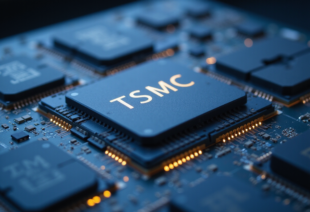
TSMC has reportedly begun pilot production of chips on its A14 process node, a 1.4nm-class technology that sits at the frontier of semiconductor manufacturing. The trial run marks the next scheduled step in the foundry's roadmap, with volume production targeted for 2028.
The A14 node follows TSMC's N2 family, the company's first process generation built on gate-all-around (GAA) nanosheet transistors. A14 extends that transistor architecture into a denser design rule set, moving from the 2nm-class dimensions of N2 to a nominal 1.4nm feature scale.
Pilot production serves a defined purpose in TSMC's development cycle. The company uses the phase to validate process recipes, yield learning, and tool sets on production-representive hardware before committing customer designs to wafer starts at scale. A successful pilot run on a next-generation node typically signals that risk production — the stage at which early customer tapeouts enter the fab — is on schedule.
According to the report, the 2028 volume production target keeps A14 on the cadence TSMC has laid out publicly. The company has described A14 as part of its continued annual-ish rhythm of leading-edge introductions, with N2 and its derivatives (N2P and N2X) carrying the 2nm generation through the mid-decade before A14 takes over at the leading edge.
The competitive context is direct. Samsung Foundry has stated plans for its own 1.4nm-class process, SF2, with a similar late-decade horizon. Intel, under its renamed process roadmap, aims to bring 14A into risk production in the same general timeframe. A14 pilot starts now give TSMC a data point in that three-way race: the earlier a node enters pilot, the greater the buffer against slippage in the path to high-volume manufacturing.
For TSMC's customers, the 2028 target matters for product planning. Chip designers working on flagship smartphone silicon, high-performance computing processors, and AI accelerators typically align their architecture roadmaps to the foundry's node schedule two to three years ahead. A node arriving in 2028 will likely power devices shipping in 2029 and beyond.
The report does not specify which fab is running the pilot lots. TSMC's leading-edge development has historically concentrated at its Hsinchu facilities in Taiwan, with subsequent volume ramps spread across sites including Fab 18 in Tainan and, for future generations, the planned Arizona complex in the United States.
Pricing follows the pattern of every recent node transition: A14 wafers will cost more than N2 wafers, which already carry a substantial premium over the preceding N3 family. Customers at the leading edge have absorbed these increases because density, performance, and power gains at each step deliver system-level value that offsets the per-wafer cost.
TSMC has not yet published full density, power, and performance figures for A14. The company typically releases those details at its technology symposiums and in updates to customers under NDA. Public disclosures so far have confirmed the node's existence, its 2028 volume target, and its position in the roadmap after N2P.
If pilot production proceeds to risk production on schedule, TSMC will move customer silicon into A14 fabs during 2027, positioning the node for a volume ramp the following year. The reported start of pilot lots keeps that sequence intact.
The report did not include yield figures for the initial pilot production. Yield maturity at pilot stage remains one of the strongest indicators of whether a 2028 high-volume target holds, and TSMC's track record on recent nodes suggests the company treats that metric as the gating item between pilot and risk production.
via Google News: TSMC (Source)
More from Priya Raman
Same lot · LOT-C1BA
- DSG-35237nmTSMC Secures Approval for Sub-1.4 nm Manufacturing Plants
- DSG-385220nmTSMC Targets 1.4nm Trial Production in Q1 2027 as Gap Widens
- DSG-163210nmTSMC Raises 2nm Output Target 20% to 120,000 Wafers Monthly
- DSG-909210nmWells Fargo Identifies Equipment Makers as 2nm Scale-Up Winners
- DSG-10203nmVSMC Opens First 12-Inch Fab in Singapore, Targeting 2027 Output