Test report DSG-3844 · Rev E · tested October 10, 2026
Memory & StorageDevice under test
Samsung's Drop-In DRAM Chip Triples AI Inference Speed
Samsung has built a DRAM chip that performs AI inference inside the memory array itself, claiming a 3x speed gain over conventional architectures and positioning the part as a drop-in memory module replacement.
- Read
- 3 min
- Words
- 553
- Node
- 10nm
- Operator
- Marcus Bennett
Spec summary
- Samsung developed a DRAM chip that performs AI inference directly within the memory array.
- Samsung describes the chip as a drop-in memory device compatible with standard module footprints.
- The company claims a threefold (3x) inference-speed improvement over conventional architectures.
- Compute logic moves from a separate processor into the DRAM die to eliminate data-movement overhead.
- Product name, capacity, interface standard, pricing, and sampling date have not been disclosed.
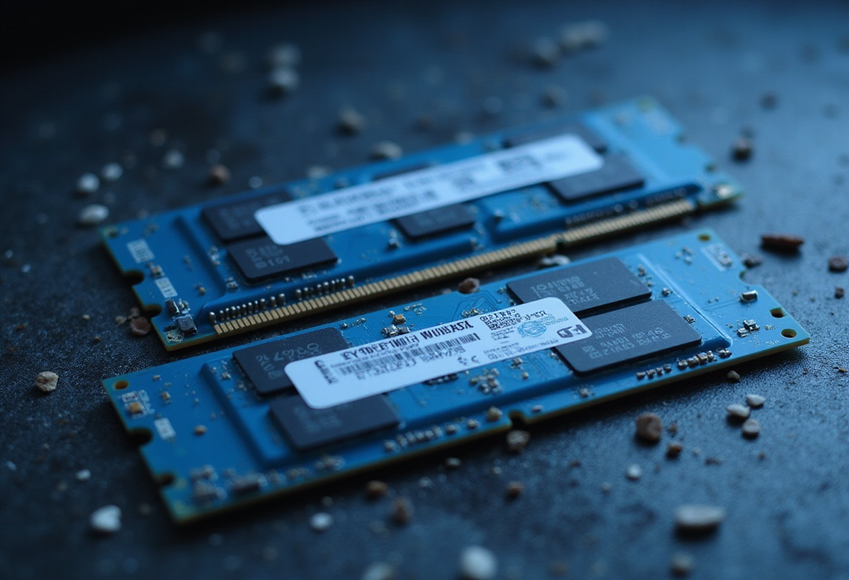
Samsung has developed a DRAM chip that performs AI inference directly within the memory array, delivering a threefold (3x) speed improvement over conventional architectures.
The part moves compute logic into the DRAM die rather than relying on a separate processor to fetch weights and activations. Samsung positions the chip as a "drop-in" memory device, indicating compatibility with standard memory interfaces that let system builders slot it into existing designs without board rework.
What does compute-in-memory change?
Conventional AI inference pipelines shuttle billions of parameters between off-chip DRAM and a separate processor. That data movement consumes most of the energy and latency budget on a typical large-model inference run. Performing multiply-accumulate operations inside the memory array itself removes the bottleneck.
A 3x inference-speed gain indicates the architecture addresses either the memory-bandwidth wall, the latency of repeated DRAM accesses, or both. The headline figure does not specify which workloads Samsung benchmarked, nor the precision or model class tested.
Why does the "drop-in" claim matter?
The drop-in framing signals that Samsung is not asking customers to redesign boards or adopt a proprietary socket. Three practical consequences follow:
- Existing module footprints appear to be retained.
- Software stacks can keep current model-loading and tensor-handling routines.
- Procurement, validation, and qualification cycles shorten for system builders.
If the part conforms to JEDEC-standard DDR or LPDDR pinouts, the addressable market expands from custom AI silicon buyers to the entire server and edge-AI memory installed base.
Where does this fit in the AI accelerator market?
Processing-in-memory has drawn sustained research attention for more than a decade. Memory vendors have published prototype PIM papers, and a limited number of HBM-based PIM products have reached sampling.
A drop-in commodity DRAM device extends the concept beyond high-bandwidth memory into standard DIMM slots used in servers, workstations, and edge-AI appliances. The shift widens the addressable market and repositions competition against three categories:
- GPU and dedicated accelerator inference pipelines from the major accelerator vendors
- High-bandwidth-memory-based PIM parts from competing memory suppliers
- Conventional DRAM modules without any compute function
A drop-in DRAM device competes less on raw throughput and more on total cost of ownership, since it can replace a standard memory module without displacing the host processor. The economics hinge on whether the embedded compute logic raises per-bit pricing by less than the savings from reduced data movement.
What remains unclear?
The available reporting does not specify:
- The product name or part number
- Capacity per module (Gb density)
- Interface standard (DDR5, LPDDR5X, HBM3, or other)
- Software support and which frameworks address the compute path
- Pricing, sampling timeline, or production volume
- Power draw at peak inference load
Until Samsung publishes a datasheet or a customer disclosure, the 3x figure functions as a benchmark claim rather than a procurement specification.
Bottom line
Samsung's compute-in-DRAM chip targets the data-movement problem that constrains large-model inference workloads. The drop-in packaging positions the part against both conventional DRAM suppliers and dedicated AI accelerators without requiring customer board redesigns.
The 3x inference-speed claim is the only quantified performance metric available. It will need independent benchmarking, full datasheet disclosure, and software-stack documentation before customers can convert it into procurement and deployment decisions.
via Google News: DRAM chip (Source)
More from Marcus Bennett
Show full bio
News editor covering marketplaces and e-commerce at Die Signal.
274 articles
Same lot · LOT-C1C6
- DSG-290728nmSamsung Operating Profit Jumps 783% to Record US$80 Billion
- DSG-698228nmMicron Earnings: AI Chip Demand Drives Fresh Memory Boom
- DSG-75607nmSamsung Forecasts HBM at 30% of DRAM Capacity by 2027
- DSG-975514nmSamsung Expects Nearly Ninefold Profit Jump on AI Memory Prices
- DSG-43067nmSamsung Q3 Operating Profit Jumps Nearly Nine-Fold on AI Chip Demand