Test report DSG-8926 · Rev A · tested November 13, 2026
Memory & StorageDevice under test
Samsung puts 46 trillion won behind HBM4E mass production
Samsung will invest 46 trillion won in Onyang HBM4E packaging, targeting June 2028 operations as it trails SK hynix in HBM and prepares a 280,000-square-meter Cheonan plant.
- Read
- 3 min
- Words
- 644
- Node
- 10nm
- Operator
- Grace Kim
Spec summary
- Samsung will invest 46 trillion won in the Onyang HBM packaging plant, with operations scheduled for June 2028.
- Samsung targets HBM4E mass production in the first half of next year and expects the product to be its flagship by 2028.
- Samsung held 33% of the HBM market in Q2 versus SK hynix's 50%; its Q3 share reached the high-30% range.
- TrendForce projects a 121% average HBM selling-price increase next year; HBM4E is expected to cost twice HBM4.
- Samsung's Chungcheong investment package totals 144 trillion won, 4 trillion won above July's 140 trillion won plan.
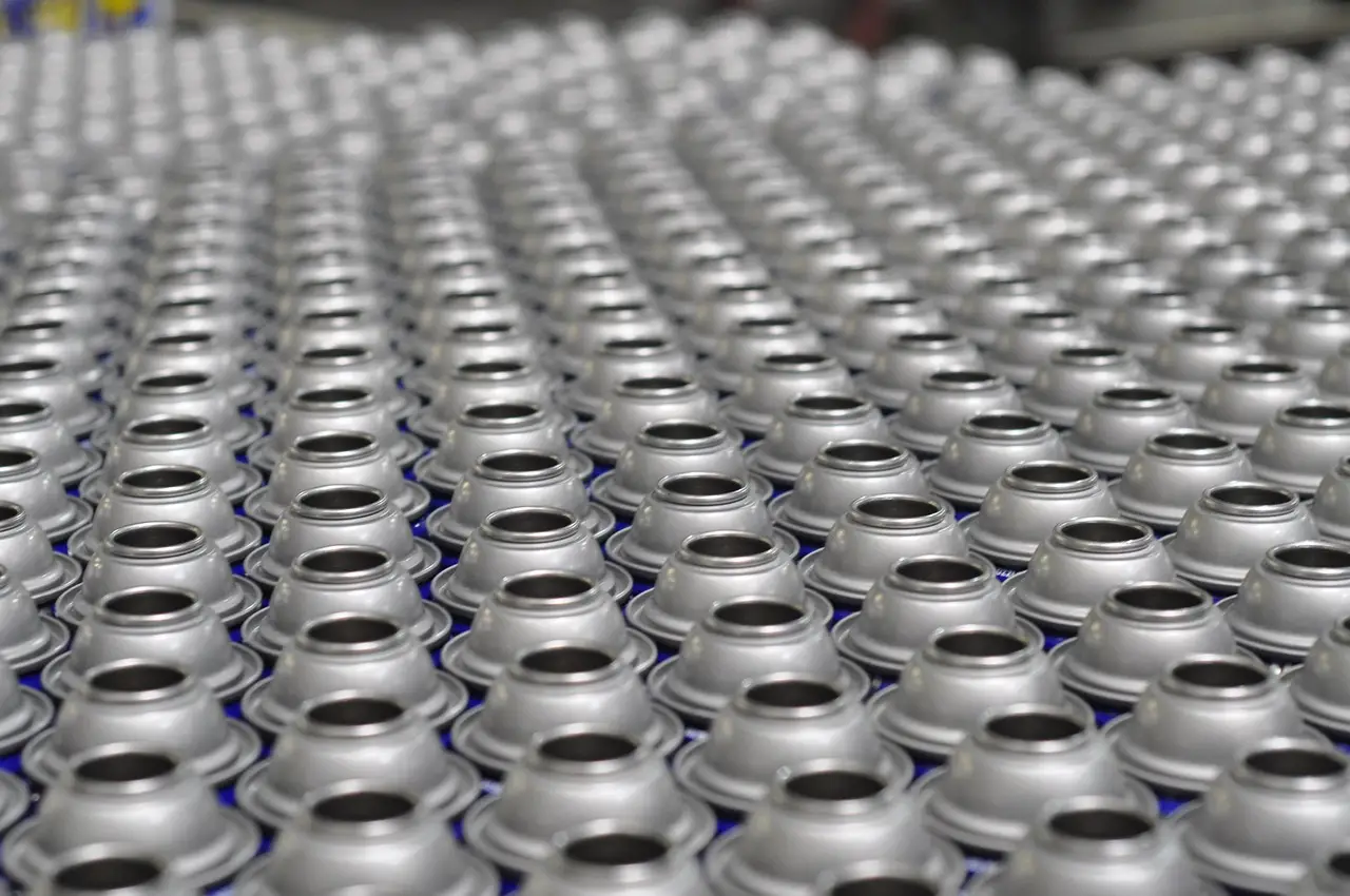
Samsung Electronics will invest 46 trillion won in a new high-bandwidth memory (HBM) packaging plant at its Onyang campus in Asan, South Chungcheong Province, with a June 2028 start scheduled for operations.
The company (005930) intends to turn Onyang into its production hub for seventh-generation HBM4E, building on its sixth-generation HBM4 program. Samsung aims to begin HBM4E mass production in the first half of next year, first in the industry, and expects the product to become its flagship by 2028.
The new line is set to expand output sharply as operations begin in June 2028, with Onyang intended to lead HBM4E production immediately after startup.
According to industry sources on the 13th, Executive Chairman Jay Y. Lee repeatedly stressed the Onyang mass-production plan to President Lee Jae-myung during the previous day's groundbreaking ceremony for the Chungcheong mega project. Samsung included an HBM4E model in a display introducing the campus's main products even though the product had not entered mass production.
President Lee signed the display with the message, “Mega Project, Korea as a Nation of Unrivaled Technology.” Samsung put HBM4E at the center of the ceremony because it sees the product as the key to reclaiming the HBM lead and widening the gap.
What does the Onyang expansion change for Samsung?
The site “has centered on simple assembly and testing of conventional chips, but will now be transformed into a hub for cutting-edge HBM, the heart of AI chips,” Lee said.
For Samsung, the practical change is the output mix: simple conventional-chip assembly and test gives way to high-value HBM packaging. Samsung wants the added capacity online as HBM4E is expected to become its flagship by 2028 and HBM5 is expected to enter mass production that year.
After Onyang, Samsung plans to expand its Cheonan campus with a 280,000-square-meter HBM packaging plant, targeted for completion at the end of next year.
Closer links with nearby dynamic random-access memory (DRAM) bases in Giheung, Hwaseong and Pyeongtaek should support a broad capacity increase for HBM4 and HBM4E, and for HBM5, which is expected to enter mass production in 2028.
The HBM market-share gap
Samsung has ceded leadership in HBM3E, the current mainstream generation, to SK hynix (000660). Samsung's HBM share stood at 33% in the second quarter of this year, against 50% for SK hynix. Its share rose to the high-30% range in the third quarter, but the gap remained around 10 percentage points.
Samsung leads the HBM4 contest, and market talk points to a possible return to the top position next year. The company is trying to pre-empt that outcome by securing HBM4E leadership before HBM4 momentum turns into a durable advantage. It also wants enough HBM4E scale to turn a possible recovery into a lasting lead.
TrendForce projects the average selling price of HBM to rise 121% next year over this year's level, driven by the HBM4 launch. HBM4E is understood to carry a price twice HBM4's. Samsung expects that mix to improve HBM profitability significantly, making HBM4E central to its effort to recover the market lead.
On the same day, Samsung announced 144 trillion won in total investment for new infrastructure in the Chungcheong region, 4 trillion won more than the 140 trillion won plan announced in July. The package covers:
- The Onyang HBM fabrication plant
- Facilities for organic light-emitting diodes
- Artificial-intelligence chip package substrates
- Next-generation battery plants
President Lee tied the expansion to the site's transformation: “Until 40 years ago, this place had nothing but barren hills and unpaved roads, but it has become an advanced plant that assembles, tests and completes semiconductors, the rice of industry.” He added: “The mega project is not merely an industrial strategy but a historic challenge that redraws the future of Korea.”
via en.sedaily.com (Source)
More from Grace Kim
Show full bio
Market editor covering regulation, policy and their impact on hardware layer of artificial intelligence at Die Signal.
565 articles
Same lot · LOT-3629
- DSG-153920nmSamsung Breaks Ground on $33 Billion HBM Packaging Push in Asan
- DSG-205165nmSamsung to Break Ground on 1.3 Trillion Won HBM Packaging Fab
- DSG-469028nmSamsung Onyang Campus to Get 46 Trillion Won for HBM Packaging
- DSG-231065nmSamsung Starts $900 Million HBM Packaging Plant in Onyang
- DSG-703145nmSamsung Raises Chungcheong Investment to 144 Trillion Won