Test report DSG-4690 · Rev A · tested November 12, 2026
Memory & StorageDevice under test
Samsung Onyang Campus to Get 46 Trillion Won for HBM Packaging
President Lee Jae-myung says Samsung's Onyang campus will gain a 6 trillion won packaging fab plus 40 trillion won in staged equipment investment for HBM packaging.
- Read
- 3 min
- Words
- 524
- Node
- 28nm
- Operator
- Priya Raman
Spec summary
- President Lee Jae-myung announced the plans on the 12th at Onyang campus in Asan.
- The Onyang site gets a 6 trillion won advanced packaging fab plus 40 trillion won in staged equipment investment.
- Three projects broke ground: packaging fab and display line in Asan, AI server substrate plant in Sejong.
- A July government-industry pledge preceded the groundbreaking by four months.
- Preparation is under way on fabs and facilities in Cheongju, Dangjin and Osong.
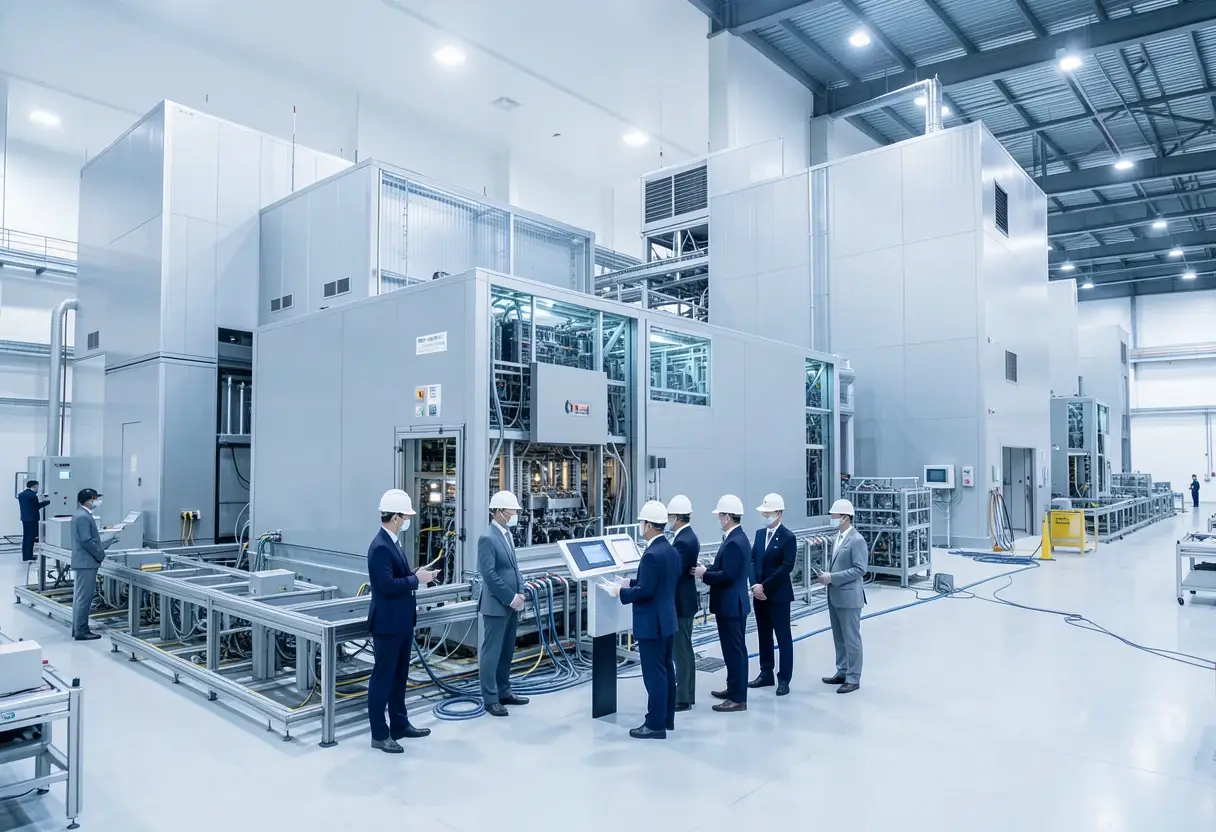
Samsung Electronics' Onyang campus in Asan will receive a 6 trillion won advanced packaging fab, followed by 40 trillion won in staged equipment investment. President Lee Jae-myung announced the figures on the 12th at the groundbreaking ceremony for the Chungcheong mega-project, held at the Onyang campus in South Chungcheong Province.
Lee said the site "will emerge as a core base for advanced HBM packaging." HBM (high bandwidth memory) is the stacked DRAM used in AI accelerators, and packaging — the process of connecting chips to substrates and each other — has become a bottleneck in AI chip supply.
What did the president announce?
Three projects broke ground simultaneously, all in the Chungcheong region:
- An advanced semiconductor packaging fab in Asan
- An advanced display production line, also in Asan
- A manufacturing facility for high-performance substrates (the layered boards that carry chips inside AI servers) in Sejong
Lee framed the ceremony as the delivery of an earlier pledge. "Last July, companies and the government stood right here in Chungcheong and promised the people a bold investment plan aimed at building an industrial powerhouse with an insurmountable lead," he said. "Just four months later, we are standing at the site where that promise is becoming reality."
The four-month gap between pledge and groundbreaking is the concrete measure here. The 46 trillion won combined figure spans the new fab and later equipment spending, and the timeline for the staged 40 trillion won tranche remains unspecified.
Where else is construction proceeding?
Lee named three additional sites where preparation is under way without disruption:
- A memory and advanced packaging fab in Cheongju
- An AI data center in Dangjin
- A biopharmaceutical production facility in Osong
"This wave of innovation is not confined to Asan and Sejong but is spreading rapidly across the entire Chungcheong region," he said. The claim covers preparation work, not completed construction, and the president gave no completion dates for any of the three sites.
Why does the Onyang investment matter?
The announcement positions the Onyang campus as a dedicated hub for HBM packaging, a segment where capacity constraints have shaped the AI supply chain. The 6 trillion won fab is the first committed tranche. The 40 trillion won equipment figure follows "in stages," which leaves the spending schedule open.
Lee said: "Here in Chungcheong today, three advanced investment projects that will redraw South Korea's industrial map are breaking ground with great momentum." Redrawing the industrial map is a political claim. The verifiable facts are the groundbreaking, the two investment figures, and the absence of stated timelines for the staged portion.
The ceremony also marks a coordination point between government and industry. The July plan Lee referenced involved both companies and the state. Whether the full 46 trillion won arrives on schedule depends on factors the address did not address: equipment lead times, demand from AI chipmakers, and the pace of the staged disbursement.
"I sincerely congratulate the people of this country on the full-scale start of construction on the Chungcheong mega-project investments," Lee said. Full-scale start applies to the three Chungcheong projects. The Cheongju, Dangjin and Osong sites remain in preparation.
via en.sedaily.com (Source)
More from Priya Raman
Show full bio
Correspondent covering money, funding and market shifts around hardware layer of artificial intelligence at Die Signal.
573 articles
Same lot · LOT-3628
- DSG-153920nmSamsung Breaks Ground on $33 Billion HBM Packaging Push in Asan
- DSG-64405nmSamsung Breaks Ground on $4.1 Billion Asan Packaging Plant
- DSG-892610nmSamsung puts 46 trillion won behind HBM4E mass production
- DSG-205165nmSamsung to Break Ground on 1.3 Trillion Won HBM Packaging Fab
- DSG-957128nmSamsung weighs 30 trillion won Giheung expansion for HBM