Test report DSG-9571 · Rev D · tested November 5, 2026
Foundries & ManufacturingDevice under test
Samsung weighs 30 trillion won Giheung expansion for HBM
Samsung may spend 25 trillion won on a four-phase Giheung fab for 2nm and 4nm HBM base dies, with dozens of EUV tools and a Line 6 advanced packaging conversion.
- Read
- 4 min
- Words
- 700
- Node
- 28nm
- Operator
- Priya Raman
Spec summary
- Samsung may invest about 25 trillion won ($18 billion) in a four-phase Giheung fab for 2nm and 4nm.
- The project total may reach 30 trillion won after converting Line 6 to advanced packaging.
- Dozens of EUV machines could account for 8 trillion won to 10 trillion won.
- Industry expects Samsung's HBM bit supply to grow 52% annually on average through 2028.
- HBM4E is scheduled to enter mass production next year using 4nm base dies.
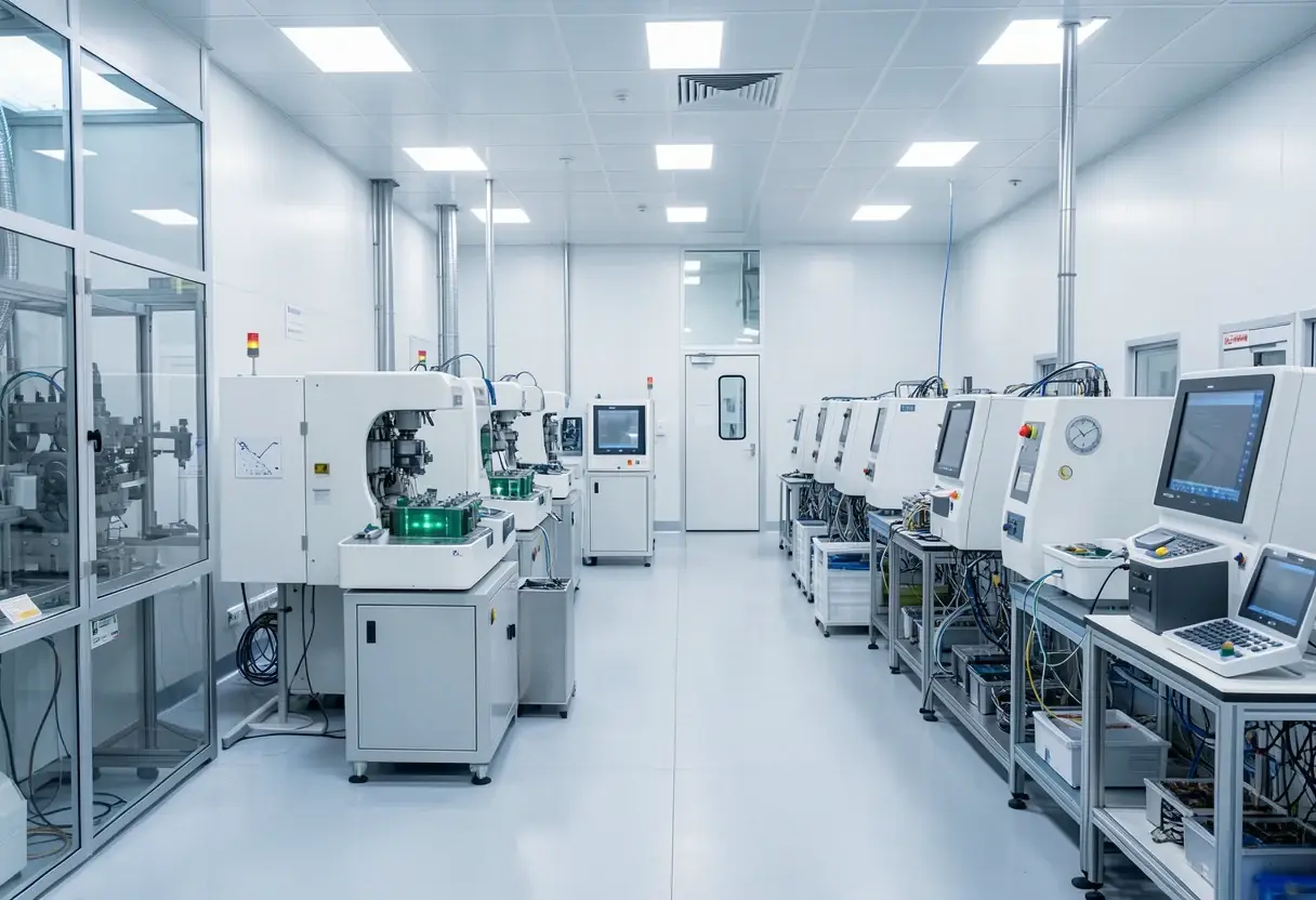
Samsung may invest around 25 trillion won (about $18 billion) in a new semiconductor fabrication plant (fab) at Giheung Campus in South Korea, according to a Sedaily report. The combined project could reach 30 trillion won after a Line 6 conversion.
The proposed site would add 2nm and 4nm capacity for high-bandwidth memory (HBM), a product assembled by stacking multiple chips. The report frames the project as support for artificial-intelligence (AI) chip supply and HBM demand from large technology firms. It identifies no customers, orders, wafer capacity or yields.
- Fab investment: around 25 trillion won, or about $18 billion.
- Possible lithography-tool allocation: dozens of machines for 8 trillion won to 10 trillion won.
- Potential total: 30 trillion won, including the Line 6 conversion.
- HBM supply forecast: 52% average annual growth in bits through 2028.
What does Samsung plan to build at Giheung?
Samsung Electronics has formed an internal task force called Kairos to turn its Giheung Campus into a production hub for 2nm and 4nm chip processes. Giheung is one of Samsung’s oldest chip campuses. The proposed fab will occupy land formerly used by the Advanced Research Institute, identified as SR5, and the College of Engineering, identified as CDI. Samsung completed demolition of both buildings in the month before the report.
Samsung E&A is slated to handle engineering, procurement and construction (EPC). The plan calls for four production phases, matching the structure of Samsung’s newest Pyeongtaek plant. The plan remains reported intent. The account gives no construction start, completion date or production timetable for Giheung.
Why does Giheung matter to HBM supply?
Samsung currently makes HBM4 core dies (the memory components) at Hwaseong and Pyeongtaek. HBM base dies (the companion components paired with those memory dies) depend on the 4nm process and come from only selected production lines. The Giheung fab could expand base-die output while keeping pace with core-die production. The account gives no wafer capacity, yield or customer allocation.
Industry expectations cited in the report put Samsung’s HBM bit supply on 52% average annual growth through 2028. That forecast measures bits, not revenue, profit or unit shipments. More output could meet large-customer demand, although no purchase commitments are disclosed.
What roles do 2nm and advanced packaging play?
Samsung uses 4nm base dies for HBM4 and the forthcoming HBM4E, which is scheduled to enter mass production next year, although no calendar year is stated. The 2nm line remains a longer-term target. HBM5 base dies are likely to use 2nm, but the report gives no HBM5 production date.
Samsung also plans to convert part of Line 6 into an advanced packaging facility. This back-end process stacks multiple chips and is important for finished HBM products. Line 6 currently handles image sensors and power semiconductors. The report does not quantify how much legacy output the conversion would displace.
How large is the investment?
The Kairos fab may involve around 25 trillion won, approximately $18 billion. Dozens of extreme-ultraviolet (EUV) lithography machines, which transfer circuit patterns onto wafers, could account for 8 trillion won to 10 trillion won. The total estimate may reach 30 trillion won with the Line 6 conversion. That figure remains conditional, and no financing plan, subsidy terms or supplier commitments appear in the report. Installation schedules and the exact number of EUV tools also remain undisclosed.
What is planned in Texas?
Samsung is also advancing a separate US expansion. The first Taylor fab in Texas is scheduled to begin mass production next year, while the company prepares to break ground on a second fab. The account provides no calendar year for that milestone, nor does it give capacity, cost or start dates for the second fab. Sedaily names no Samsung executive and quotes none.
The Giheung proposal remains a reported plan with an estimated total and no disclosed customer commitments. The plan links 4nm base dies to HBM4 and HBM4E, and likely 2nm base dies to HBM5. Advanced packaging would perform the stacking step, while industry expects Samsung’s HBM bit supply to grow 52% annually through 2028. Missing data prevent a firmer assessment of construction timing, tool delivery, yields, customer commitments and production allocation.
via Google News: AI chip (Source)
More from Priya Raman
Show full bio
Correspondent covering money, funding and market shifts around hardware layer of artificial intelligence at Die Signal.
573 articles
Same lot · LOT-360C
- DSG-55437nmSamsung's Giheung HBM expansion could cost 30 trillion won
- DSG-703145nmSamsung Raises Chungcheong Investment to 144 Trillion Won
- DSG-153920nmSamsung Breaks Ground on $33 Billion HBM Packaging Push in Asan
- DSG-204610nmAI Chip Capacity Race Pushes Vietnam Deeper Into Semiconductor Chain
- DSG-160614nmSamsung Readies Groundbreaking on Second Major Chip Plant