Test report DSG-9550 · Rev C · tested November 11, 2026
Foundries & ManufacturingDevice under test
Samsung Hands Used Metrology Tool and Fab Know-How to Public Nanofab
Samsung transferred an 8-inch thin-film metrology tool to the Korea Advanced Nano Fab Center in Suwon, plus fab operating know-how, under a March 2024 government MOU with three chipmakers.
- Read
- 3 min
- Words
- 586
- Node
- 65nm
- Operator
- Marcus Bennett
Spec summary
- Samsung transferred an automated 8-inch thin-film measurement system to the Korea Advanced Nano Fab Center in Suwon, announced on the 11th.
- Consulting ran from June to October, following an MOU signed in March last year with Samsung, SK hynix and DB HiTek.
- Samsung developed its first site inspection manual adapted for public nanofabs, based on one used at mass-production facilities.
- The program adapted Samsung's supplier-support consulting into SOPs, checklists and training standards for each tool.
- The government plans to expand consulting and idle-equipment transfers across MOA-Fab institutions.
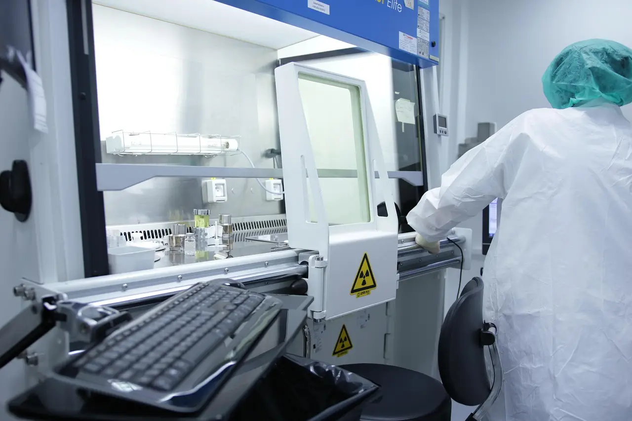
Samsung Electronics has transferred an automated thin-film pattern measurement system to a public nanofabrication center in Suwon, handing over both equipment and fab operation know-how to the state-run research infrastructure.
The Ministry of Science and ICT announced the transfer on the 11th at a ceremony held at the Korea Advanced Nano Fab Center. The event also reported results of a consulting project between Samsung and the center on improving public nanofab operations, and marked the handover of used equipment to MOA-Fab, the platform that links and integrates public nanofabs across the country.
Where does the know-how come from?
The transfer follows a memorandum of understanding signed in March last year between the ministry and three chipmakers: Samsung Electronics, SK hynix and DB HiTek. Samsung's Device Solutions division win-win cooperation center ran consulting at the Korea Advanced Nano Fab Center over four months, from June to October, after similar work at the National Nanofab Center and the Nano Convergence Technology Center.
The consulting adapted a program Samsung already runs for its own semiconductor materials, parts and equipment suppliers. The output was concrete: standard operating procedures for each tool, plus checklists, training standards and operating standards reflecting the center's fab operation and management practices.
Samsung also developed and applied, for the first time, a site inspection manual tailored to public nanofabs. The manual adapts one previously used only at mass-production private facilities. It sets out standard procedures that let institutions monitor fab safety and equipment conditions on an ongoing basis rather than through occasional checks.
What does the equipment do?
The transferred tool is an automated thin-film pattern measurement system. It measures single- and multi-layer film thickness and optical constants on 8-inch semiconductor wafers, using a non-destructive method that supports process monitoring. The government expects the handover to give the center a new 8-inch automated thin-film metrology capability it did not previously have.
The Korea Advanced Nano Fab Center plans to use the system for research and development and for technical support to companies, universities and research institutes. It will operate the tool alongside its existing fab services and specialist training programs.
What does this change for the ecosystem?
Ji Hyun-ki, executive vice president and head of the win-win cooperation center at Samsung's Device Solutions division, framed the program as a loop between private and public sectors. "We want to help build a virtuous cycle of shared growth, in which the manufacturing innovation know-how Samsung Electronics has accumulated flows through public nanofabs back to researchers and to materials, parts and equipment companies," he said. "We will continue to take part as the consulting model developed this time spreads to other institutions participating in MOA-Fab, contributing to stronger competitiveness in the domestic semiconductor ecosystem."
Koo Hyuk-chae, first vice minister of science and ICT, said global semiconductor competition has shifted into a contest that mobilizes the full capabilities of nations. That makes public-private cooperation, which channels private equipment and know-how into public research infrastructure, increasingly important.
"We will expand cooperation models such as private-sector consulting and transfers of idle equipment across institutions participating in MOA-Fab, raising the overall operating standards of public nanofabs and actively supporting semiconductor technology innovation and the training of skilled professionals," Koo said.
The ministry's stated goal is to extend the model beyond Suwon. Institutions linked through MOA-Fab are the next candidates for both consulting and idle-equipment transfers.
via en.sedaily.com (Source)
More from Marcus Bennett
Show full bio
News editor covering regulation, policy and their impact on hardware layer of artificial intelligence at Die Signal.
591 articles
Same lot · LOT-3627
- DSG-205165nmSamsung to Break Ground on 1.3 Trillion Won HBM Packaging Fab
- DSG-153920nmSamsung Breaks Ground on $33 Billion HBM Packaging Push in Asan
- DSG-957128nmSamsung weighs 30 trillion won Giheung expansion for HBM
- DSG-822820nmSamsung Staffs Up Taylor Fab as 2nm Production Nears
- DSG-36305nmSamsung Table 260 Billion USD National Semiconductor Complex Plans