Test report DSG-5740 · Rev E · tested October 30, 2026
Memory & StorageDevice under test
Micron Skips G10: G11 NAND Passes 400 Layers, Doubles Density in 2027
Micron drops its planned 300-plus-layer G10 NAND and jumps to a 400-plus-layer G11 node with wafer-on-wafer bonding, doubling density and lifting the interface to 5,400 MT/s by late 2027.
- Read
- 4 min
- Words
- 755
- Node
- 3nm
- Operator
- Amara Osei
Spec summary
- G11 NAND exceeds 400 layers and doubles bit density to ~42 Gb/mm², ramping in H2 2027
- Interface speed rises from 3,600 MT/s to 5,400 MT/s; energy per bit drops more than 25%
- Micron skips the planned G10 node of more than 300 layers; G9 has 276 layers today
- HBM4 36GB 12-high parts entered mass production in March 2026; HBM6 follows in 2030
- New SLC-based drives target up to 100 million random reads per second and 512TB capacities
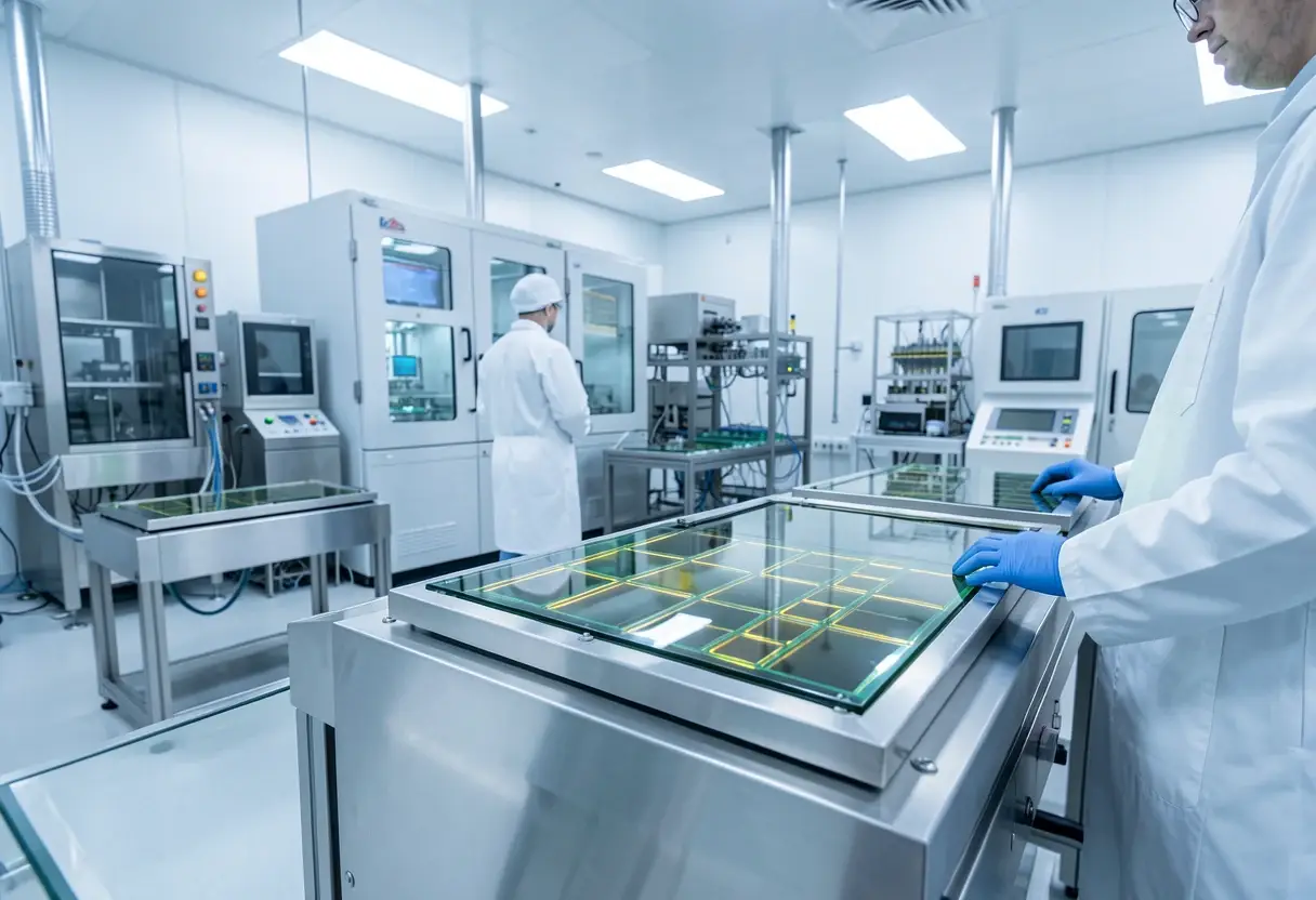
Micron will jump from its current 276-layer G9 NAND straight to a G11 node with more than 400 layers, roughly double the bit density and a 50% faster interface, with volume production set for the second half of 2027. The Boise, Idaho-based chipmaker announced the plan at a technology and product webinar on Oct. 21.
Scott DeBoer, Micron's president and chief technology and products officer, said G11 is built on wafer-on-wafer bonding: the memory array and peripheral logic are fabricated on separate wafers with different process technologies, then joined. Micron has used CMOS-under-array designs for several generations; bonding lets it tune the array and supporting circuitry independently.
"This G11 technology is the world's most advanced NAND," DeBoer said. "It will ramp in the second half of next year, [and] it is based on wafer-on-wafer bonding technology."
What are the stated G11 targets?
- Bit density (3D TLC): about 42 Gb/mm², up from about 21 Gb/mm² on G9
- Interface speed: 5,400 MT/s, up from 3,600 MT/s
- Energy per bit transferred: more than 25% lower than G9
- Layer count: more than 400, versus 276
- Bonding: wafer-on-wafer, replacing CMOS-under-array
Micron has not disclosed active wordline counts, memory decks or cell dimensions. The company says only that the cell pitch will lead the industry, implying density gains come from both extra layers and smaller cells.
Why skip a generation?
The skip is unusual. Micron had been expected to ship a G10 part with more than 300 layers first; that step is dropped. Its NAND progression now runs from 32 layers in the first generation through 176 layers, 232 layers (G8) and the 276-layer G9, which ships in products such as the 2650 client SSD launched in July 2024.
DeBoer said the memory was deliberately reworked for coming AI workloads, which drove the G9-to-G11 jump rather than a step-by-step cadence. Micron is positioning the node for two new storage classes:
- A high-IOPS, SLC-based product targeting 25 million to 100 million random reads per second, with next-generation drives reaching up to 512TB.
- A high-bandwidth NAND that stacks dies connected through silicon vias to a base die, similar in concept to high-bandwidth memory, placed near accelerators rather than at the package edge.
"Because we think it doesn't make sense to put it on the coastline of the accelerator, [we place it] closer to the compute itself to take advantage of this high-performance NAND," DeBoer said. Such parts will cost more and require co-development with customers to hit performance and cost targets.
He did not address high-bandwidth flash, a similar stacking concept promoted by SanDisk and SK hynix.
Beyond G11, Micron is developing high-mobility materials, denser cell architectures and lower-energy data paths to keep shrinking NAND in all three dimensions. "Beyond G11, we have a strong roadmap, not going to go into great detail on it today, but really focused on new materials densifying the cell architecture, and continuing to focus on that XYZ scaling going forward," DeBoer said. More G11 technical details arrive in 2027, closer to manufacturing start.
What did the broader roadmap add?
The NAND update came alongside briefings on DRAM and HBM. BNP Paribas senior equity research analyst Karl Ackerman said Micron told subscribers that HBM4 36GB 12-high parts entered mass production in March 2026, HBM4E is sampling with major customers with mass production planned for 2027, and HBM5 follows in 2028, HBM5E in 2029 and HBM6 in 2030.
Micron also disclosed vertical HBM, placing DRAM stacks directly above a processor, and vertical edge inference memory, which puts low-power LPDDR above logic; both target 2028 production, with three generations planned by 2030. Ackerman noted Micron is shifting from in-house HBM4 base dies to foundry-supplied base dies for HBM4E to meet speed and power targets, and will offer custom HBM with customer logic IP in the base die alongside JEDEC-standard products for the first time.
NAND pricing and layer counts remain a competitive scoreboard: Samsung, SK hynix and the Kioxia-SanDisk alliance each roll out successive generations. Skipping G10 compresses Micron's timeline but raises execution risk — wafer bonding is new to its NAND lines, and the company promises density, speed and power gains simultaneously. For data-center buyers, doubled density at a 50% faster interface would cut cost per terabyte and ease power and space constraints in AI clusters.
via Google News: HBM memory (Source)
More from Amara Osei
Show full bio
Staff writer covering money, funding and market shifts around hardware layer of artificial intelligence at Die Signal.
507 articles
Same lot · LOT-C204
- DSG-302545nmMicron G11 NAND Doubles Density, Hits 5,400 MT/s in 2H 2027
- DSG-959345nmMicron Targets NVIDIA Custom HBM Standards in TSMC Partnership
- DSG-397414nmMicron Sets New Revenue and Profit Records on Sustained AI Demand
- DSG-65503nmMicron Bets on Wafer Bonding and High-NA EUV for Post-4F2 DRAM
- DSG-510065nmMicron ends 2GB GDDR7 production, shifts 3GB silicon to AI GPUs