Test report DSG-3025 · Rev B · tested October 30, 2026
Memory & StorageDevice under test
Micron G11 NAND Doubles Density, Hits 5,400 MT/s in 2H 2027
Micron's G11 3D NAND doubles bit density to ~42 Gb/mm², pushes I/O to 5,400 MT/s and cuts per-bit transfer energy 25%+, ramping in 2H 2027.
- Read
- 3 min
- Words
- 647
- Node
- 45nm
- Operator
- Elena Vasquez
Spec summary
- G11 3D NAND enters mass production in 2H 2027 with over 400 layers
- Bit density roughly doubles versus G9: ~21 Gb/mm² to ~42 Gb/mm² 3D TLC
- I/O speed rises 50%, from 3,600 MT/s to 5,400 MT/s; per-bit transfer energy drops over 25%
- G11 adopts wafer-on-wafer bonding, building the array and peripheral logic on separate wafers
- Post-G11 roadmap relies on new materials and XYZ cell scaling; details due in 2027
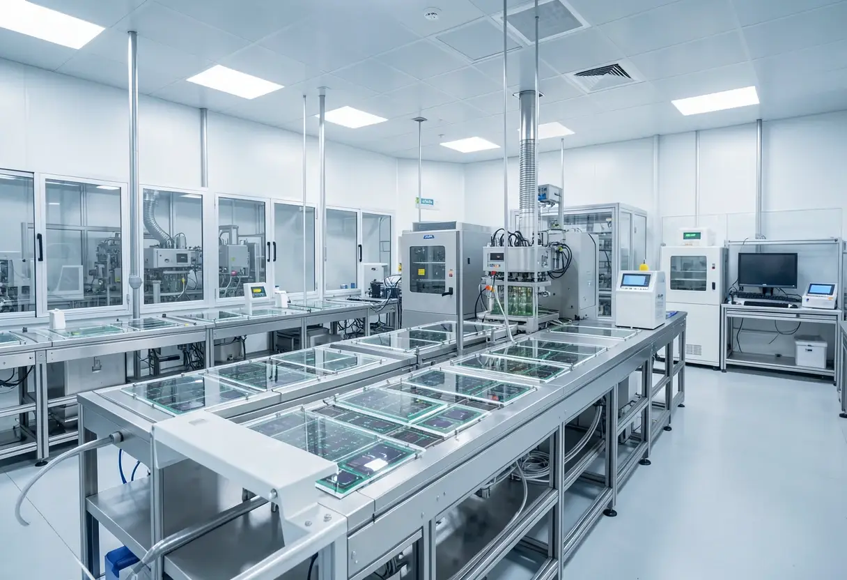
Micron's G11 3D NAND will double bit density to roughly 42 Gb/mm² and lift I/O speeds by 50% to 5,400 MT/s when it enters mass production in the second half of 2027. The company laid out the roadmap at an event this week, and the numbers put clear air between Micron and its two closest rivals on density — well beyond what Kioxia's BiCS10 or Samsung's V10 currently offer.
For drive makers and buyers, that means client and data center SSDs with more capacity per die, plus the bandwidth and efficiency headroom that AI-oriented storage devices increasingly demand. G11 also cuts data transfer energy per bit by more than 25%, which matters when you're moving data at multi-gigabit interface speeds all day.
What changes with wafer bonding?
The headline architectural shift is wafer-on-wafer bonding — a technique YMTC pioneered in commercial NAND. Micron builds the NAND array on one wafer using a new 3D NAND node, fabricates peripheral circuits and I/O on a separate wafer using a logic process, then bonds the two together.
Scott DeBoer, Micron's president and chief technology and products officer, framed the timing as a cost decision, not a technology stunt: "We had mentioned we will bring in wafer-on-wafer bonding technology at the right time when it's cost-effective, and it brings in capability that is important for the product specs at the time, and this is the right timing for that technology." He added: "So this G11 technology is the world's most advanced NAND. It will ramp in the second half of next year, [and] it is based on wafer-on-wafer bonding technology."
Micron has used CMOS-under-array for several generations, so decoupling array and logic isn't new territory conceptually. What changes is flexibility: each side can now be optimized independently, which translates directly into more capacity and performance — if yields cooperate.
How does 400-plus layers fit in?
G11 moves past 400 NAND layers, up from the current G9 (N160) generation. Micron hasn't disclosed the exact count of active wordline layers or the number of memory decks, so treat the 400 figure as a floor, not a spec.
On density: G9 3D TLC sits around 21 Gb/mm², and G11 targets roughly double that. On speed, the interface jumps from 3,600 MT/s to 5,400 MT/s. The company also claims an industry-leading memory cell pitch, which signals the gains come from both added layers and shrunk cell dimensions rather than stacking alone.
Expect fuller technical disclosures in 2027, closer to high-volume manufacturing.
What comes after G11?
Micron isn't planning to scale by layer count alone. Future generations will also shrink cells along the X and Y axes — denser packing in the horizontal plane, not just taller stacks. The company points to three workstreams: high-mobility materials, ultra-dense cell architectures, and more energy-efficient devices and data paths.
DeBoer kept the post-G11 roadmap vague but directionally clear: "Beyond G11, we have a strong roadmap, not going to go into great detail on it today, but really focused on new materials densifying the cell architecture, and continuing to focus on that XYZ scaling going forward." He continued: "The current industry direction and Micron's direction is scaling both by adding layers [and] also by shrinking the cell dimensions."
No density targets, architectural details, or production schedules for post-G11 generations have been disclosed. Still, since adding layers remains the easiest lever for density, expect the layer-count race to keep running — especially with demand for 3D NAND-based storage staying strong.
For practitioners, the practical takeaway is a timeline: plan around G11-based products reaching volume in 2H 2027, with density and bandwidth gains that should ripple into SSD pricing and capacities well after that.
via Tom's Hardware (Source)
More from Elena Vasquez
Show full bio
Senior reporter covering people, launches and day-to-day practice in hardware layer of artificial intelligence at Die Signal.
498 articles
Same lot · LOT-C204
- DSG-57403nmMicron Skips G10: G11 NAND Passes 400 Layers, Doubles Density in 2027
- DSG-65503nmMicron Bets on Wafer Bonding and High-NA EUV for Post-4F2 DRAM
- DSG-750314nmMemory supply tightens around AI demand, Equiti analysis shows
- DSG-210510nmSK hynix Reportedly Lags Samsung in HBM Hybrid Bonding
- DSG-98875nmSamsung: HBM to Take 30% of DRAM Wafer Capacity by 2027