Test report DSG-3639 · Rev F · tested November 14, 2026
Memory & StorageDevice under test
KAIST Team Maps 3D Current Paths in RRAM, Finds Electrode Bumps Steer Filaments
KAIST researchers reconstructed RRAM conductive pathways in 3D and found electrode surface protrusions steer filament growth, pointing to a new design lever for memory stability.
- Read
- 3 min
- Words
- 538
- Node
- 28nm
- Operator
- Elena Vasquez
Spec summary
- KAIST team observed RRAM current pathways in 3D using conductive atomic force microscopy
- A 10-nanometer titanium dioxide layer was shaved in ~0.1-nanometer steps over 100 rounds
- All five observed pathways connected to nanometer-scale protrusions on the platinum electrode
- Findings published online in Nano Letters on Aug. 11; announced by KAIST on the 12th
- First author: Park Gun-woo, combined master's-doctoral student at KAIST
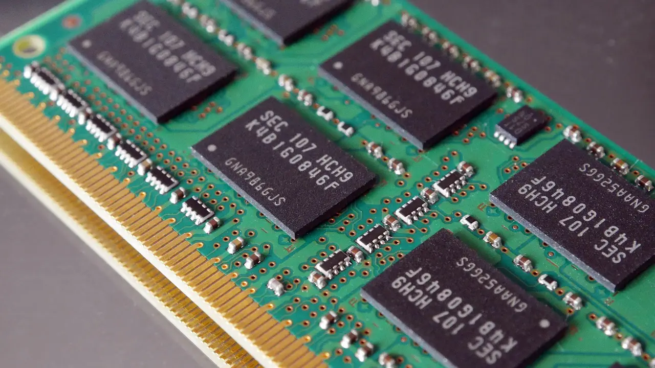
Engineers at KAIST have reconstructed the interior of a resistive random-access memory (RRAM) cell in three dimensions and found that nanometer-scale protrusions on the electrode surface dictate where and in which direction conductive pathways grow. The Korea Advanced Institute of Science and Technology announced the result on the 12th, from a joint team led by professors Hong Seung-bum and Park Sang-hee of the Department of Materials Science and Engineering. The paper appeared online in Nano Letters on Aug. 11, with combined master's-doctoral student Park Gun-woo as first author.
Why does this matter for RRAM design?
RRAM stores bits by forming or breaking conductive pathways — a filament that conducts reads as one value, a broken one as the other. It's nonvolatile, structurally simple, and a candidate both for next-generation storage and for neuromorphic AI chips that process information brain-like.
The long-standing problem is variability. When pathways form at inconsistent locations or in inconsistent shapes, the voltage needed to write or erase data shifts from operation to operation, undermining device stability. Until now, nobody had adequately explained what governs a pathway's growth direction or the exact point where it connects.
How did the team see inside the device?
They used conductive atomic force microscopy as a nanoscale milling machine. The team shaved away a titanium dioxide layer — 10 nanometers thick, roughly 50 times thinner than a single virus shell — in about 0.1-nanometer increments over 100 rounds, measuring the current distribution at each depth. Stacking those measurements produced a full 3D reconstruction of the internal pathways.
The geometry was consistent. Each pathway formed an inverted cone: wide near the upper probe, narrowing toward the lower electrode. Crucially, the tip of each pathway connected to nanometer-scale protrusions on the lower platinum electrode rather than to flat regions. All five pathways formed at different locations showed the same pattern.
Computer simulations backed the mechanism. Electric field concentration appeared around the upper probe and around the protrusions on the lower electrode, supporting the conclusion that field hotspots at surface bumps steer filament growth.
What changes for practitioners?
The study goes beyond structural observation and ties pathway geometry to a controllable manufacturing variable. If designers treat the electrode surface — not just the switching layer — as a design parameter, precisely shaping and positioning protrusions could anchor pathways at consistent locations.
"This study is meaningful in that it goes beyond simply observing the three-dimensional shape of conductive filaments and understands their form and the position of their tips in connection with the actual nanostructure of the electrode," Hong said.
The design implication is direct. "If the electrode surface structure is also treated as a design variable, it will serve as an important foundation for developing next-generation resistive memory that operates more stably," he added.
For RRAM and neuromorphic chip developers, that means variability control may shift from switching-layer engineering toward electrode surface finishing — a process variable fabs already know how to tune. The 3D characterization method itself, layer-by-layer tomography at 0.1-nanometer resolution, also offers a reusable tool for diagnosing filament behavior in other resistive devices.
The findings were published in Nano Letters on Aug. 11.
via en.sedaily.com (Source)
More from Elena Vasquez
Show full bio
Senior reporter covering people, launches and day-to-day practice in hardware layer of artificial intelligence at Die Signal.
589 articles
Same lot · LOT-362A
- DSG-384410nmSamsung's Drop-In DRAM Chip Triples AI Inference Speed
- DSG-65503nmMicron Bets on Wafer Bonding and High-NA EUV for Post-4F2 DRAM
- DSG-634220nmCXMT Reports Architecture Breakthrough in Memory Chips
- DSG-526020nmChina's 4F² DRAM claim puts Samsung and SK Hynix on notice
- DSG-97267nmGelsinger Calls HBM 'Hideous Memory' as DRAM Shortages Run to 2028