Test report DSG-7962 · Rev C · tested November 5, 2026
Foundries & ManufacturingDevice under test
Intel Says EMIB Wafer Utilization Tops 90% as AI Chips Push Bridge Counts Past 70
Intel reported EMIB wafer utilization above 90% versus 60% for interposers at ISMP 2026, as AI packages head toward 240x240mm with more than 70 bridges and Google and Amazon emerge as EMIB-T customers.
- Read
- 3 min
- Words
- 604
- Node
- 5nm
- Operator
- Amara Osei
Spec summary
- Intel reported EMIB bridge wafer utilization above 90%, versus about 60% for interposer-based packaging, at ISMP 2026 in Busan on November 4.
- AI packages commercialized in 2026 reach 120x120mm with 12 HBM stacks and over 20 bridges; future 240x240mm packages are projected to need more than 70 bridges.
- Google's TPU v9 designs HumuFish and TriggerFish are expected to use EMIB-T, while WhaleFish will use TSMC's CoWoS-L; Amazon is also reportedly adopting EMIB-T.
- TrendForce projects TSMC's CoWoS-L will grow from 5.5 reticles with four chiplets in 2026 to 14 reticles with 20 chiplets and 20 HBM stacks by 2028.
- UMC produces EMIB silicon bridges on mature 12-inch processes at fabs in Taiwan and Singapore.
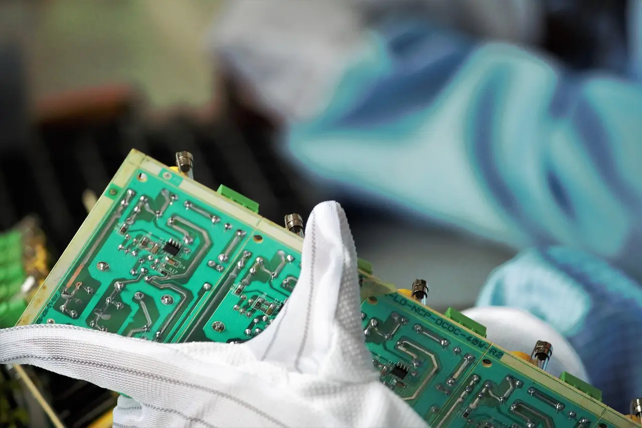
Intel reported a wafer utilization rate above 90% for its EMIB bridge packaging process on November 4, against roughly 60% for the silicon interposer approach, positioning the technology as a cost-efficient challenger to TSMC in the 2.5D packaging market.
Lee Kyu-oh, a director overseeing packaging at Intel Foundry, presented the figures at ISMP 2026 (International Symposium on Microelectronics Packaging), held at the Paradise Hotel in Busan, South Korea. EMIB — Embedded Multi-die Interconnect Bridge — connects dies by placing small silicon bridges only at necessary points, rather than a large silicon interposer supporting the entire chip. The bridge approach wastes far less silicon per package.
The takeaway: EMIB converts a structural choice into a cost argument, with a roughly 30-point utilization gap over interposers.
What is EMIB-T and why does it matter?
EMIB-T, the variant drawing the most industry attention, embeds through-silicon vias (TSVs) inside the bridges to secure power delivery paths.
"EMIB-T is an architecture that can flexibly respond to demands for larger chips by placing high-density silicon only where needed," Lee said. "Considering AI semiconductor performance, embedding TSVs in all bridges will become the trend."
The implication: as AI silicon grows, Intel expects TSV-bearing bridges to become the default, not an option.
Which customers are lining up?
Customer acquisition is taking concrete shape, according to industry sources:
- Among Google's TPU v9 lineup, HumuFish and TriggerFish are expected to use Intel's EMIB-T.
- WhaleFish, the third TPU v9 design, will use TSMC's CoWoS-L.
- Amazon is reportedly planning to adopt EMIB-T for its own AI chips.
The takeaway: Intel has named-level design-win momentum at two hyperscalers, though Google is splitting its TPU family between foundries.
How large are the packages getting?
The trend toward larger AI chips directly multiplies bridge demand. Lee's presentation laid out three tiers:
- Commercialized in 2026: packages up to 120x120mm, up to 12 HBM stacks, more than 20 EMIB bridges.
- Under development: 120x180mm or larger, at least 16 HBM stacks, more than 38 bridges.
- Future outlook: 240x240mm packages with more than 32 HBM stacks, pushing required bridges past 70.
The takeaway: bridge counts roughly triple as package area quadruples, and each bridge is a unit of demand Intel can capture.
Who supplies the bridges?
Growing bridge volume also reshapes Intel's supply chain. The silicon bridges for EMIB are produced by Taiwan-based foundry UMC using mature 12-inch processes at its fabs in Taiwan and Singapore, according to the report.
The takeaway: EMIB scaling depends on mature-node capacity at UMC, not on leading-edge wafer supply.
How does TSMC respond?
TSMC is pursuing larger AI packages through its CoWoS family. Market research firm TrendForce projects that CoWoS-L will integrate four chiplets and 12 HBM stacks in a 5.5-reticle-size package in 2026. By 2028, TrendForce expects CoWoS-L to reach 14 reticles, accommodating 20 chiplets and 20 HBM stacks.
Industry observers say Intel's EMIB family is emerging as a realistic alternative while TSMC's CoWoS production capacity remains tight.
The takeaway: capacity scarcity at TSMC, not outright technical superiority, is opening the door for Intel.
What could still go wrong?
Two conditions will decide whether EMIB converts into mass-production volume, according to industry observers: securing design wins from major customers and achieving back-end process yields. The customer pipeline — Google's TPU v9 designs and Amazon's AI chips — addresses the first condition on paper. Yields at scale remain unproven.
The takeaway: Intel has the utilization numbers and the customer names; yield is the unresolved variable.
via Google News: AI chip (Source)
More from Amara Osei
Show full bio
Staff writer covering money, funding and market shifts around hardware layer of artificial intelligence at Die Signal.
593 articles
Same lot · LOT-360C
- DSG-758665nmSK Hynix Details Advanced Packaging for Next-Gen HBM
- DSG-40957nmSK Hynix Taps Intel EMIB-T for Next-Gen HBM Packaging
- DSG-239414nmTSMC taps U.S. interposers to speed AI chip packaging shift
- DSG-414414nmTSMC and GlobalFoundries Tie Up $2 Billion on US Advanced Packaging
- DSG-90903nmNvidia Reportedly Eyes Intel Packaging, Easing TSMC's Backend Load