Test report DSG-2955 · Rev D · tested October 26, 2026
Memory & StorageDevice under test
Custom HBM Set to Fully Open Next Year, Reshaping Memory Alliances
Custom HBM opens fully next year, with Samsung and SK Hynix co-designing memory for NVIDIA and Google — and weighing TSMC-built base dies that could erode their design and production control.
- Read
- 3 min
- Words
- 617
- Node
- 20nm
- Operator
- Elena Vasquez
Spec summary
- The custom HBM market is expected to fully open next year.
- NVIDIA unveiled NVHBM in August, moving memory control circuits into the base die.
- Ahn Hyun, SK Hynix Head of Development, predicted custom HBM will dominate in an October 14 SEDEX keynote.
- Samsung is considering manufacturing NVIDIA base dies at TSMC.
- Custom HBM commands higher prices than standard HBM due to complex design requirements.
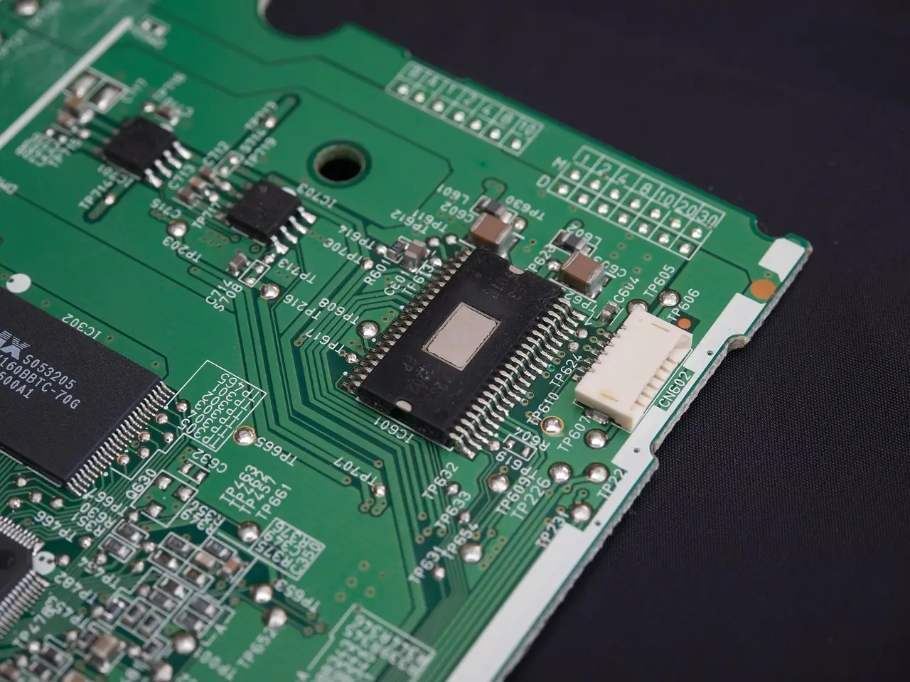
The market for custom high-bandwidth memory will fully open next year, ending the era in which memory makers sold one standardized HBM product to every customer. From 2026 onward, Samsung Electronics and SK Hynix will co-develop memory designs from the earliest stage to match each customer's AI chip architecture. Competition shifts with it: no longer just capacity and speed, but the performance and power efficiency of entire AI systems.
That shift is redrawing collaboration structures across the industry. AI chip developers such as NVIDIA and Google now participate in HBM's internal design, while memory companies contribute to logic design — including customer-specific control circuits that go beyond DRAM. Companies coordinate design, processes and packaging from early development, rather than just connecting separately produced chips.
What is custom HBM, concretely?
Custom HBM is memory tailored to the structure and purpose of a customer's AI semiconductor. The critical component is the base die, which sits at the bottom of the stacked DRAM layers and exchanges data with the external AI chip. Think of HBM as an apartment building: the upper floors store data, and the base die is the first floor with the door to the street.
Custom HBM embeds customer-specific functions and connection methods into that base die to optimize data transfer performance and power efficiency.
How does NVIDIA's NVHBM change the workflow?
NVIDIA's NVHBM, unveiled in August, shows the new mechanics. Its core innovation moves the memory control circuit — previously part of the AI accelerator — into the base die. That means Samsung and SK Hynix must collaborate with NVIDIA on base die design while strengthening their own logic design capabilities for customer-specific circuits.
Production routes may shift too. Samsung is considering manufacturing NVIDIA's base dies at TSMC — its competitor — to meet specific requirements. Design houses, memory companies and foundries now coordinate design and production from the early stages to optimize for each customer's AI chips.
Where's the money?
For memory makers, custom HBM opens a higher-value market. It commands higher prices than standard versions because of complex design requirements and additional features. As big tech firms like Google and Amazon expand their application-specific integrated circuit (ASIC) development, demand for custom HBM optimized per chip should grow.
Ahn Hyun, SK Hynix's Head of Development (President), said during a keynote at the Semiconductor Exhibition (SEDEX) on October 14: "While standard and custom HBM will coexist, the custom trend will eventually dominate."
Who controls the design — and the fab?
The risks sit in two places. First, design leadership. Memory firms previously designed base dies and allocated circuits on their own. Custom HBM requires joint decisions on how much space customer-specific circuits get. If a customer demands more room, memory companies must squeeze their own circuits into narrower areas — raising design complexity and potentially forcing finer processes.
A semiconductor industry source put it plainly: "Semiconductors are ultimately about how many circuits can fit into the smallest space. If customer circuits occupy more area in the base die, memory companies must compress their own circuits into tighter spaces."
Second, production leadership. If AI chip developers like AMD and Broadcom also request TSMC processes for their base dies, memory companies may increasingly outsource production of core components even while winning HBM orders. Samsung, which runs its own foundry, could face constraints linking HBM orders to internal foundry capacity. Memory makers' HBM production schedules may also grow more dependent on TSMC's capacity and allocation.
Analysts suggest memory firms must balance standard and custom HBM production ratios based on profitability per customer — and on how much dependency on any single client or foundry they're willing to accept.
via Google News: HBM memory (Source)
More from Elena Vasquez
Show full bio
Senior reporter covering people, launches and day-to-day practice in hardware layer of artificial intelligence at Die Signal.
466 articles
Same lot · LOT-C1EB
- DSG-96247nmSamsung to outsource custom DRAM, redirect fabs to HBM for AI
- DSG-44375nmNvidia Co-Designs Custom HBM With Samsung and TSMC, Targets 30% More Bandwidth
- DSG-59533nmAnalysts: HBM Memory Cut Samsung Losses by 41% in a Year
- DSG-166610nmSamsung to Detail Evolving HBM Base Die at Hot Chips 2026
- DSG-809520nmSK hynix commits $13 billion to world's largest HBM assembly plant