Test report DSG-9674 · Rev E · tested October 10, 2026
Memory & StorageDevice under test
SK hynix approves $38.3bn for two memory fabs in South Korea
SK hynix's board has approved a $38.3bn capital plan for a DRAM fab at the Yongin cluster and a NAND expansion on an existing South Korean campus, with first cleanrooms due in December 2028 and June 2029.
- Read
- 3 min
- Words
- 623
- Node
- 5nm
- Operator
- Grace Kim
Spec summary
- SK hynix approved $38.3bn for two fabs on 13 August 2026
- Yongin Y2 DRAM fab: 279 acres, construction starts July 2027, first cleanroom June 2029
- NAND flash facility: first cleanroom December 2028, on a campus already hosting three fabs
- Investment sits within South Korea's $880bn national semiconductor and AI infrastructure plan
- Follows March 2026 announcement of an AI-driven autonomous fab targeting 2030 operation
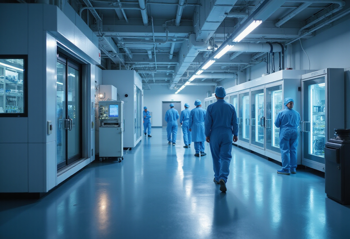
SK hynix's board approved a $38.3 billion capital programme on 13 August 2026 to fund two new semiconductor fabs in South Korea: a DRAM plant at the Yongin Semiconductor Cluster and a separate NAND flash facility at an existing manufacturing campus.
The commitment forms part of South Korea's wider $880bn national plan for semiconductors, physical AI and AI data centres, under which both SK hynix and Samsung Electronics will build multiple fabs at the new Yongin hub south of Seoul.
Combined, the two new fabs represent one of SK hynix's largest recent commitments to production infrastructure. First cleanrooms at the sites are targeted for December 2028 and June 2029. Market impact will ripple across the cleanroom construction supply chain through the end of the decade.
What will Yongin Y2 produce?
Yongin Y2 will be the second of four semiconductor fabs SK hynix plans at the Yongin cluster. The company said construction will start in July 2027 and that the first cleanroom will reach operational status in June 2029.
The facility will run DRAM production lines, including high-bandwidth memory (HBM) used in AI accelerators and high-performance computing systems. Once complete, it will span 279 acres of floor space — a footprint that places it among the largest individual memory fabs now under development worldwide.
HBM has become a key revenue driver for SK hynix as NVIDIA, AMD and custom AI silicon customers consume stacked DRAM dies for GPU and accelerator packages.
What does the NAND flash site add?
The NAND flash facility will rise on a campus already home to three operational fabs. SK hynix said existing power and water infrastructure at the site will support and accelerate the build programme, with the first cleanroom due to open in December 2028 — roughly six months ahead of the DRAM schedule.
This sequencing positions NAND capacity additions to arrive first, followed by DRAM and HBM output growth from Yongin. The NAND site sits within an established SK hynix manufacturing cluster, which the company has flagged as a logistical advantage for cleanroom fit-out, chemical delivery and ultrapure water distribution.
How does the plan fit SK hynix's wider roadmap?
Key specifications across the two projects:
- Yongin Y2 (DRAM/HBM): construction start July 2027; first cleanroom June 2029; 279 acres of floor space
- NAND flash facility: first cleanroom December 2028; located on a campus with three existing fabs
- Total approved capital: $38.3bn
- National programme: South Korea's $880bn semiconductor and AI infrastructure plan
- Earlier 2026 commitment: autonomous AI-driven fab target for 2030 operation
In March 2026, SK hynix announced plans for an AI-driven autonomous fab to be operational by 2030. That facility will integrate AI, robotics and digital-twin control systems within next-generation cleanroom environments. The announcement set a benchmark for high-automation memory manufacturing in Asia.
What does the move mean for the cleanroom supply chain?
The Yongin Semiconductor Cluster sits southwest of Seoul. Both SK hynix and Samsung Electronics plan to operate multiple fabs there under the national framework, concentrating memory and logic production in a single regional hub.
The $38.3bn authorisation extends a multi-year demand cycle for high-specification cleanroom construction, ultrapure water systems, chemical delivery networks and HVAC infrastructure across Korean semiconductor sites. Korean cleanroom contractors, gas and chemical delivery specialists, and process tool vendors can expect project pipelines running through 2029 and beyond, with significant demand for ISO Class 3 and Class 4 environments to support advanced DRAM and 3D NAND process nodes.
The Yongin site has already entered cleanroom fit-out at SK hynix's first fab, with central chemical supply system installation underway ahead of 2027 production. The Y2 approval accelerates the next build phase on the same campus.
via hpcimedia.com (Original)
More from Grace Kim
Same lot · LOT-C1C6
- DSG-410110nmSK Hynix Commits $38 Billion to Two New DRAM and NAND Plants
- DSG-71977nmSK Hynix Commits $38 Billion to Korean Chip Fab Expansion
- DSG-106210nmSK Hynix weighs US chip manufacturing, Taipei Times reports
- DSG-67193nmSK Hynix Eyes Opportunity Inside Intel's $100B U.S. Fab Plan
- DSG-16585nmSK Hynix commits $720 billion to AI-fueled South Korea buildout