Test report DSG-9997 · Rev F · tested November 7, 2026
Memory & StorageDevice under test
Samsung's Second Texas Plant to Build HBM Base Dies for AMD and Nvidia
Maeil Business Newspaper reports Samsung's second Taylor, Texas fab will make 2nm HBM base dies for AMD and Nvidia, fully booked, with production in 2030. Samsung declined comment.
- Read
- 3 min
- Words
- 597
- Node
- 45nm
- Operator
- Priya Raman
Spec summary
- Samsung's second Taylor, Texas plant will produce HBM base dies for AMD and Nvidia, Maeil reported November 3.
- The fab spans about 2.7 million square feet, 1.5 times the first Taylor plant, and uses 2nm technology.
- Equipment installation is slated for February 2029, with mass production in 2030.
- Most of the fully booked output reportedly goes to AMD; the first plant serves Tesla.
- Samsung Electronics declined to comment.
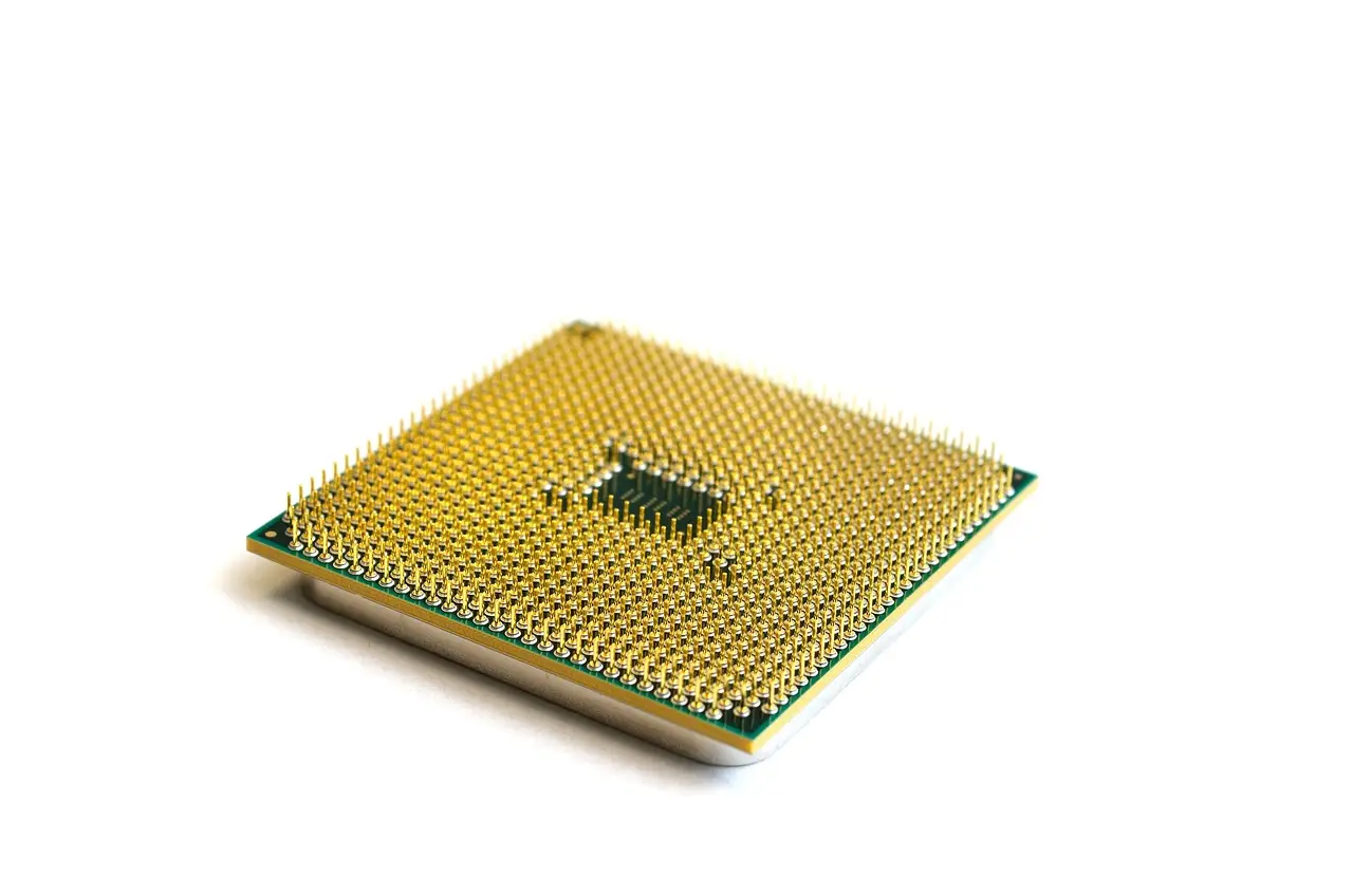
Samsung Electronics will produce base dies (the silicon layer beneath a memory stack that routes signals) for high-bandwidth memory chips at its second foundry plant in Taylor, Texas, according to a report published Tuesday, November 3, by South Korea's Maeil Business Newspaper. The report cites unnamed industry sources. AMD and Nvidia are named as the customers.
Samsung Electronics declined to comment on the matter. That refusal matters. Every claim in the story rests on one outlet's anonymous sourcing, and neither AMD nor Nvidia has confirmed the orders.
What does the Taylor plant claim to deliver?
The details, as reported by Maeil, are specific:
- Formal construction begins this month, November 2025.
- The plant has secured orders for its entire output.
- Most of the secured volume is for AMD, not Nvidia.
- The fab will run 2-nanometre process technology (a measure of transistor scale; smaller means denser, faster chips).
- The facility covers roughly 2.7 million square feet, about 1.5 times the size of the first Taylor plant.
- Equipment installation starts in February 2029; mass production follows in 2030.
The size comparison offers the only concrete anchor: 2.7 million square feet is roughly half the floor area of the Pentagon. Maeil notes the first Taylor facility holds a contract with Tesla.
Why do base dies matter?
High-bandwidth memory, or HBM (memory chips stacked vertically to feed AI processors at high speed), depends on base dies to connect the stack to a customer's GPU or accelerator logic. Producing those dies on a 2nm node at scale would place Samsung inside the supply chain for two of the largest AI chip designers in the United States. That is the market significance. It is also, at present, a projection five years out.
A single anonymous-source report claiming full capacity sold before construction formally starts invites scrutiny, because foundries rarely disclose customer allocation and neither AMD nor Nvidia has verified the split that Maeil describes. The 2030 mass-production date gives every party ample room to revise, delay, or cancel without breaching any public commitment.
What remains unconfirmed?
Three gaps stand out.
First, no financial terms appear in the report. Neither the value of the orders nor the pricing of the wafers is disclosed. Second, the AMD-versus-Nvidia volume split is described only as "most" for AMD. No percentage, wafer count, or revenue figure supports that characterization. Third, the production timeline hinges on equipment installation in February 2029, an event more than three years away.
Reuters contributed to the reporting through journalists Joyce Lee and Heekyong Yang, with editing by Kirsten Donovan, but the wire service attributed all substantive claims to Maeil.
What is the practical takeaway?
If the report holds, Samsung gains a fully booked advanced-node fab on US soil, serving the two dominant AI accelerator vendors while its first Taylor plant serves Tesla. For AMD, a reported majority share of the capacity would secure domestic base-die supply for its HBM stacks. For Nvidia, the arrangement would add a second-source option alongside existing suppliers.
Those conditionals carry weight. Samsung's decision not to deny the report is not confirmation, and the company has previously revised timelines on US foundry projects without penalty or explanation. The 2.7-million-square-foot plant, the 2nm process node, the February 2029 equipment date, and the 2030 production start all remain claims from a single Korean newspaper citing sources nobody can check.
Die Signal will track whether Samsung, AMD, or Nvidia issues on-record confirmation, and whether the November construction start proceeds as described.
via Google News: HBM memory (Source)
More from Priya Raman
Show full bio
Correspondent covering money, funding and market shifts around hardware layer of artificial intelligence at Die Signal.
573 articles
Same lot · LOT-360E
- DSG-807065nmSamsung Plans 2nm HBM Base Die Production in Texas From 2030
- DSG-737514nmSamsung to Start Building Second Taylor Chip Plant Next Month
- DSG-62523nmSamsung Sets November Groundbreaking for Second Taylor Fab
- DSG-487220nmSamsung to Build Taylor Fab 2 in 2025, Locks 70% Memory Capacity
- DSG-828214nmSamsung to Use TSMC Technology for Nvidia's Next-Gen Memory Chips