Test report DSG-1824 · Rev A · tested October 15, 2026
Edge AI SiliconDevice under test
Samsung's Exynos 2800 Could Be First Mobile Chip With HBM Memory
Samsung's Exynos 2800 could become the first mobile SoC to integrate High Bandwidth Memory, according to Android Headlines. Samsung has not commented publicly on the report.
- Read
- 3 min
- Words
- 541
- Node
- 45nm
- Operator
- Priya Raman
Spec summary
- Android Headlines reports the Exynos 2800 could be the first mobile SoC to integrate HBM memory
- HBM stacks multiple DRAM dies vertically using through-silicon vias, delivering higher bandwidth than LPDDR
- Current flagship mobile SoCs typically reach 50 to 100 GB/s through LPDDR5X memory
- HBM stacks in data-center configurations deliver 200 to 800 GB/s depending on generation
- Exynos 2400 shipped in 2024 inside Galaxy S24 series devices in select markets
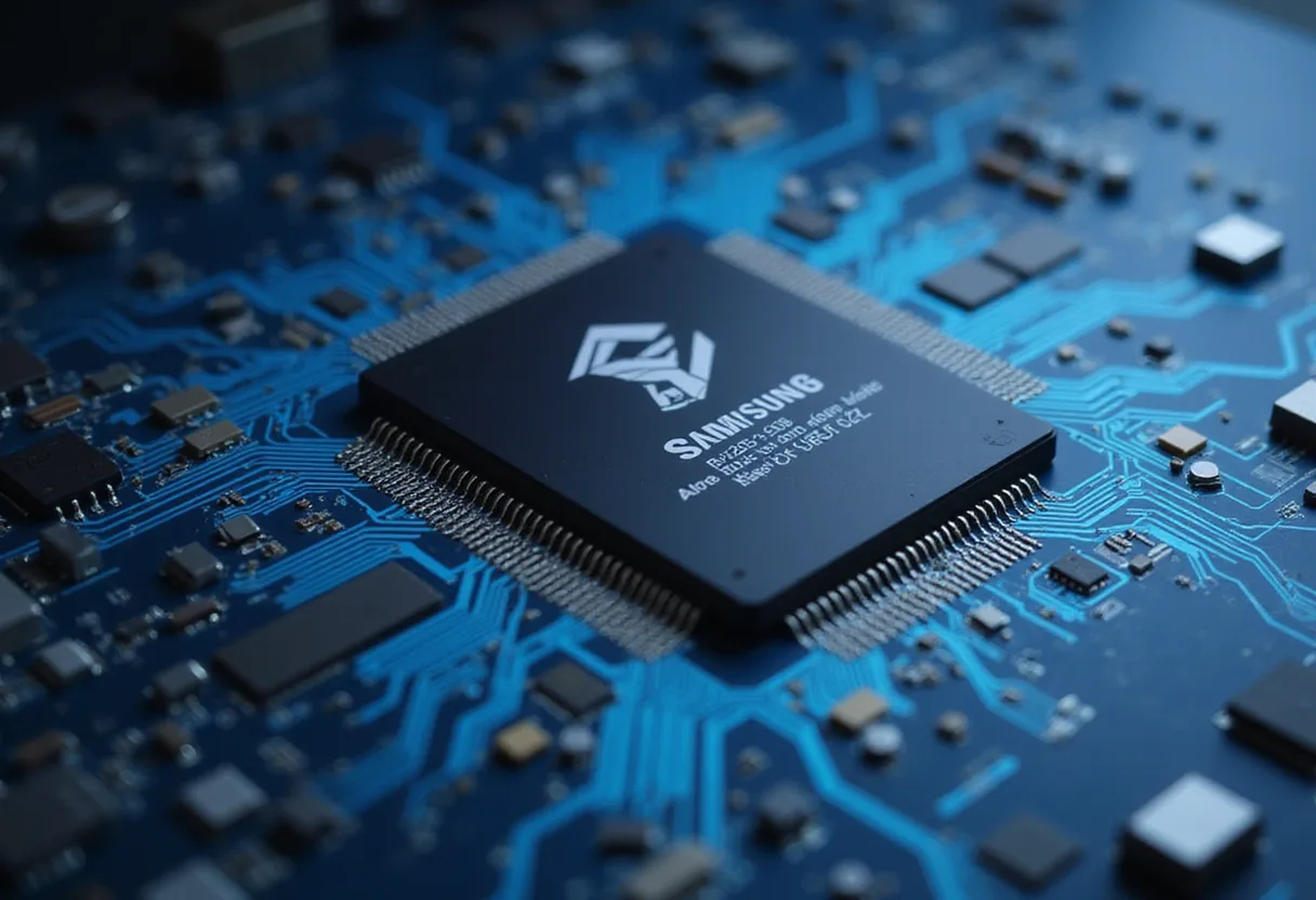
Samsung's Exynos 2800 could become the first mobile system-on-chip (SoC, a chip integrating CPU, GPU and other accelerators on one die) to integrate HBM (High Bandwidth Memory), according to Android Headlines. The publication's headline frames the chip as "the First Mobile Chip to Use HBM for Powerful On-Device AI."
The Exynos line is Samsung's in-house mobile processor family, used in Galaxy smartphones and other devices. Samsung has not officially confirmed the Exynos 2800 name, specifications, or launch window. Android Headlines has not disclosed the basis for its reporting.
What does HBM bring to a mobile processor?
HBM stacks multiple DRAM dies vertically using through-silicon vias (TSVs), short electrical pathways that pierce the silicon between layers. The architecture delivers higher bandwidth than the LPDDR (Low Power Double Data Rate) memory that dominates current mobile designs. HBM reduces energy per transferred bit, but demands a larger footprint and more complex package than LPDDR.
Why does on-device AI require higher memory bandwidth?
Large language models and multimodal AI workloads move vast parameter sets between compute units and memory. Bandwidth, not raw clock speed, typically determines inference speed for transformer-class neural networks (the layered architecture underlying modern generative AI).
Running such models locally requires moving tens to hundreds of gigabytes per second through the memory channel, a sustained throughput that current LPDDR5X implementations approach but rarely exceed in commercial handset designs. Current flagship mobile SoCs offer 50 to 100 GB/s through LPDDR5X, a specification of LPDDR memory in its fifth major revision. That ceiling constrains local model size.
HBM stacks deliver 200 to 800 GB/s in data-center configurations, depending on generation. Even a constrained mobile variant would likely clear thresholds for running mid-sized generative models locally.
What remains unconfirmed?
Several parameters remain unspecified in the Android Headlines piece, leaving readers unable to verify the technical and commercial claims without additional sourcing from the chipmaker or its suppliers. The report does not state:
- The chip's manufacturing node (the fabrication geometry, such as 3 nm or 2 nm)
- The HBM generation in use (HBM2, HBM3, HBM3E, or HBM4)
- Production timeline or commercial release window
- Die size, transistor count, or thermal envelope (maximum sustained power dissipation)
Samsung has not commented publicly. The company's most recently confirmed flagship mobile chip, the Exynos 2400, shipped in 2024 inside Galaxy S24 series devices in select markets.
What would substantiation require?
Independent confirmation typically arrives from supply-chain analysts tracking foundry and packaging allocations, or from Samsung's own investor disclosures. Mass-production HBM in a mobile package would require either a new external packaging partner or additional capacity within Samsung's existing advanced packaging facilities.
HBM has historically cost three to five times more per gigabyte than conventional LPDDR, a multiple that would raise the bill of materials (total component cost) for any adopting handset. That cost delta would push adoption toward premium tiers first, if the technology arrives at volume.
Until Samsung addresses the report, the claim should be treated as an unverified leak. The underlying technical premise aligns with sustained industry pressure to shift inference workloads from remote cloud servers onto client devices, a transition driven by latency, privacy and operating-cost considerations.
via Google News: HBM memory (Source)
More from Priya Raman
Show full bio
Correspondent covering money, funding and market shifts around hardware layer of artificial intelligence at Die Signal.
369 articles
Same lot · LOT-C1CB
- DSG-75607nmSamsung Forecasts HBM at 30% of DRAM Capacity by 2027
- DSG-59533nmAnalysts: HBM Memory Cut Samsung Losses by 41% in a Year
- DSG-91507nmSamsung Secures 70% of HBM Memory Capacity Through 2031
- DSG-87827nmSamsung Passes HBM4E Qualification with Nvidia and Major Hyperscalers
- DSG-362314nmSamsung to Detail Evolving HBM Base Die at Hot Chips 2026