Test report DSG-3623 · Rev B · tested November 18, 2026
Processors & AcceleratorsDevice under test
KAIST Moves Clock Mesh to Backside Metal in BSPDN Chip Design
KAIST researchers placed a clock mesh on backside metal layers shared with BSPDN, solving receiver placement with a potential-field method.
- Read
- 2 min
- Words
- 485
- Node
- 45nm
- Operator
- Amara Osei
Spec summary
- KAIST published the paper as arXiv:2611.20414 in November 2026, under a CC BY 4.0 license.
- The design moves the clock mesh to backside metal layers shared with the BSPDN, leaving the rest of the network on the frontside.
- A potential-field method solves mesh receiver placement under keep-out zones between clock- and power-nTSVs.
- Authors Kim, Chae, Zhang and Shin will present at ASPDAC'27 in Tokyo, January 25–28, 2027.
- The ACM version spans 7 pages with DOI 10.1145/3840404.3848262.
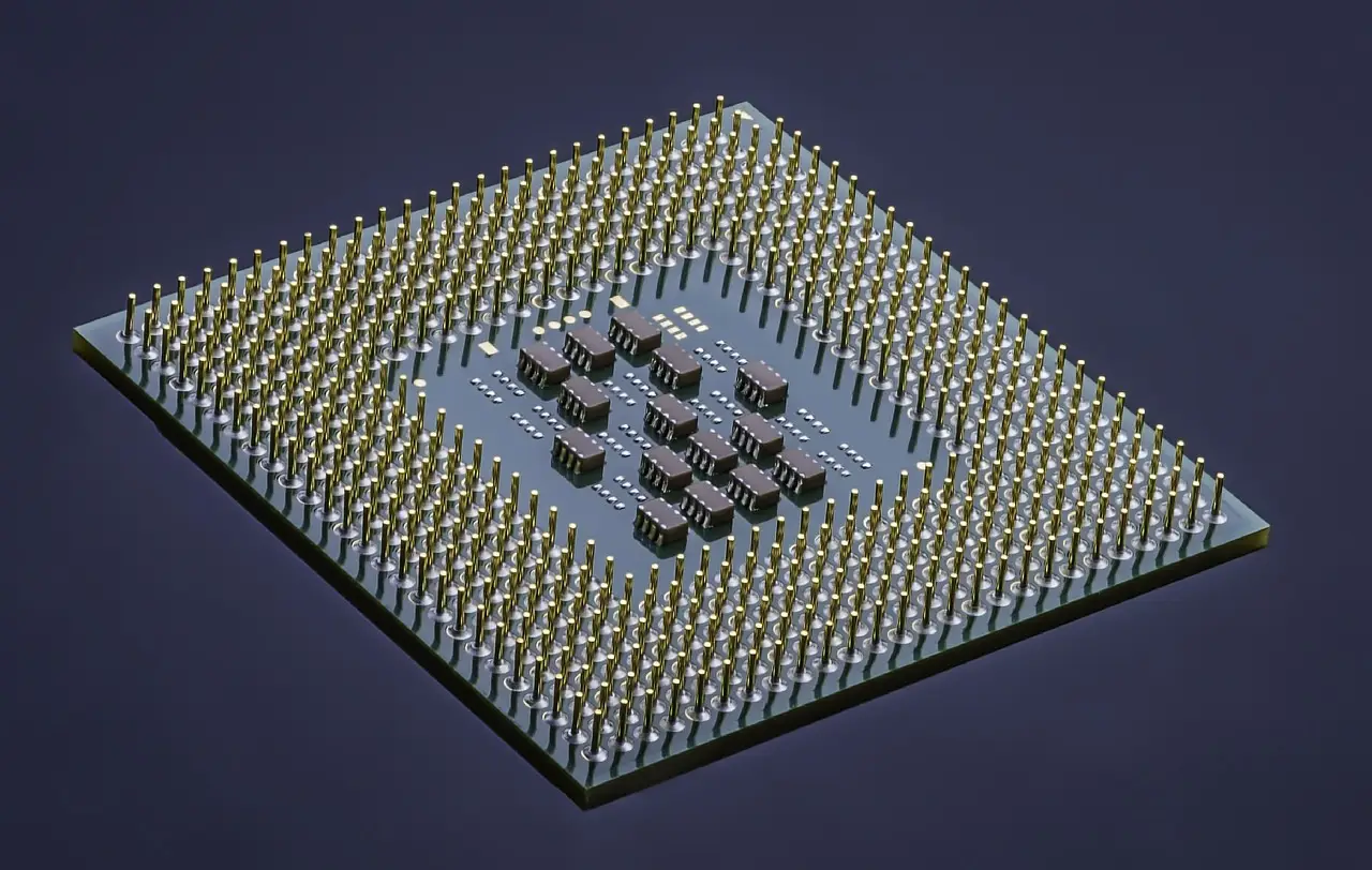
Researchers at the Korea Advanced Institute of Science and Technology (KAIST) published a clock distribution network design on November 2026 that places the clock mesh on backside metal (BM) layers — the same layers already claimed by the backside power distribution network (BSPDN). The paper, "Clock Distribution Network with Backside Clock Mesh in BSPDN Architecture," carries the identifier arXiv:2611.20414 and is licensed CC BY 4.0.
The four authors — Seohyun Kim, Youngjin Chae, Shilong Zhang and Youngsoo Shin — will present the work at the 32nd Asia and South Pacific Design Automation Conference (ASPDAC'27), scheduled for January 25–28, 2027 in Tokyo, Japan. ACM will publish the seven-page paper with the DOI 10.1145/3840404.3848262.
What does the design change?
The proposal splits the clock distribution network (CDN) across two sides of the die. The clock mesh moves to the backside metal layers. The remainder of the network stays on the frontside. According to the authors' abstract, this split directly addresses two figures of merit in clock delivery: skew and power.
The arrangement creates an immediate resource conflict. Because the BSPDN also occupies the backside metal layers, the clock mesh and the power network must share that real estate. Routing both signals through the same layers is the central constraint the paper works around.
The authors state the problem plainly in the abstract:
"Since the backside power distribution network (BSPDN) also uses the BM layers, the clock mesh and power network must share them."
How do the researchers solve mesh placement?
The paper identifies a specific placement task: positioning mesh receivers while respecting keep-out zones (KOZs) that must sit between clock-nTSVs and power-nTSVs — the through-silicon vias that carry each signal type through the backside stack. Place a receiver inside a keep-out zone and the two via populations interfere.
The authors report that a potential-field method (PFM) solves this placement problem. The abstract states:
"We show that this problem can be solved using a potential-field method (PFM)."
A potential-field method treats the keep-out zones as repulsive regions and guides mesh receivers toward legal positions, an approach the KAIST team applies to the shared backside layers.
Why does backside clocking matter now?
Backside power delivery has moved from research topic to roadmap item across the advanced-node logic segment, and the KAIST paper extends that infrastructure beyond power. Sharing the backside metal between the power network and a clock mesh means the frontside layers carry less routing burden, and the paper's title claims the technique reduces both skew and power in the resulting clock tree.
The work stands as a concrete step in that direction: a full clock distribution scheme, a defined placement problem, and a named algorithmic solution, documented across seven pages and accepted at a peer-reviewed design automation venue.
Readers can retrieve the technical paper at arxiv.org/abs/2611.20414.
via arxiv.org (Original)
More from Amara Osei
Show full bio
Staff writer covering money, funding and market shifts around hardware layer of artificial intelligence at Die Signal.
698 articles
Same lot · LOT-362E
- DSG-58235nmKorean V-Die and Japanese MOSAIC designs reorient HBM stacks to cut heat
- DSG-776120nmTSMC Reportedly Pulls 1.4nm Production Forward to April 2027
- DSG-30167nmSynopsys Certifies A14 EDA Flow with TSMC; 64G UCIe Hits 2nm/3nm
- DSG-62407nmTSMC Targets 1.4nm Trial Production in Q1 2027 as Gap Widens
- DSG-660528nmTSMC's Chipmaking Edge Bolsters Wei's Leverage Into Musk's Terafab