Test report DSG-9130 · Rev A · tested November 4, 2026
Foundries & ManufacturingDevice under test
TSMC A16 Targets 2027 Volume Production Ahead of Intel, Samsung
TSMC says its 1.6-nanometer-class A16 process delivers 8-10% more performance or 15-20% lower power than N2P, with volume production targeted for 2027, ahead of Intel 14A and Samsung SF1.4.
- Read
- 4 min
- Words
- 829
- Node
- 3nm
- Operator
- Priya Raman
Spec summary
- TSMC targets A16 production readiness in 2026 and volume production in 2027.
- A16 claims 8-10% faster performance or 15-20% lower power than N2P, plus roughly 8-10% higher transistor density.
- High-NA EUV systems cost more than €350 million each; A16 will use TSMC's existing EUV fleet.
- Intel plans 14A risk production in the second half of 2027 and high-volume production in 2028; Samsung targets SF1.4 mass production in 2029.
- TSMC plans to more than double annual N2-family capacity in 2027.
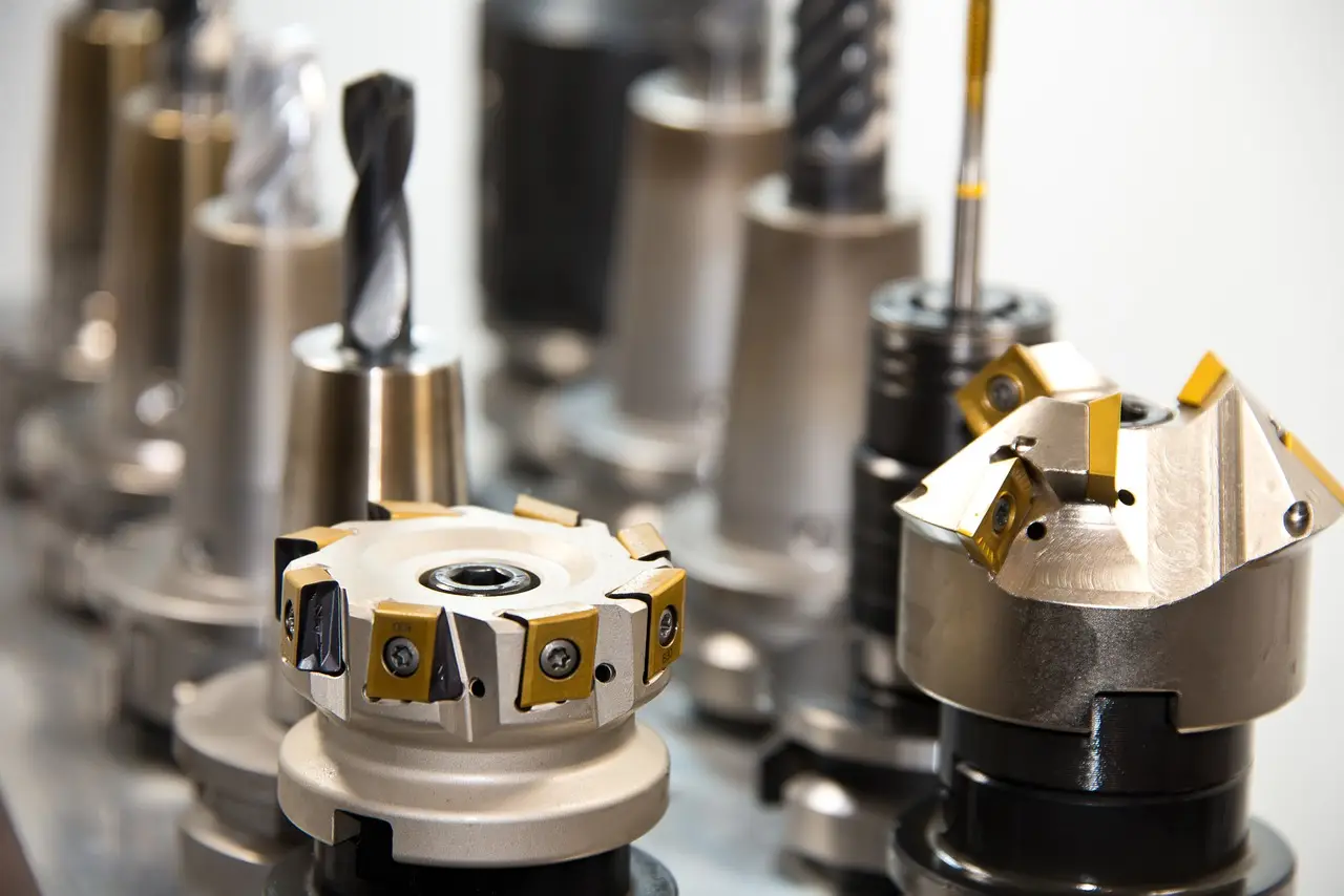
TSMC expects its A16 process to reach volume production, meaning large-scale commercial manufacturing, in 2027 after production readiness in 2026. The 1.6-nanometer-class node targets high-performance computing (HPC) products with complex signal routing and dense power-delivery networks. Customer product ramps also point to 2027.
What performance does A16 claim?
TSMC reports three gains over its N2P process:
- 8% to 10% faster performance at the same power draw.
- 15% to 20% lower power consumption at the same speed.
- Roughly 8% to 10% higher transistor density.
These remain company claims. The source provides no independent benchmark, production yield, customer chip or A16 volume allocation.
A16 will become TSMC's first process to use what the company calls Super Power Rail, moving the power-delivery network to the wafer's back instead of routing it beside signal wires on the front. The practical target is power savings for AI accelerators, which run hot around the clock. That benefit remains unverified at production scale.
Why is TSMC avoiding High-NA?
TSMC says it will reach those targets without ASML's high-numerical-aperture extreme-ultraviolet (High-NA EUV) tools. Each system costs more than €350 million.
TSMC instead extracts the gains through its existing EUV fleet and process engineering. A TSMC executive identified only as Zhang said at an earlier node briefing: "I like the technology but I don't like the sticker price." The remark addresses acquisition cost, not manufacturing output or defect rates.
Intel made the opposite equipment bet. It became the first chipmaker to receive ASML's High-NA system. Intel plans to use that tool in 14A production.
On the stated schedules, TSMC approaches volume production without High-NA before Intel expects to employ the tool, illustrating that node execution rather than equipment ownership determines the lead.
How do the roadmaps compare?
Intel CEO Lip-Bu Tan said this year that the company has fully committed to high-volume 14A production in 2028. Risk production, meaning early manufacturing used to test a design, starts for internal chips in the second half of 2027. This accelerates Intel's position from one year earlier, when it warned that it might abandon 14A without a major external customer.
Samsung's SF1.4 node does not target mass production until 2029. That is two years later than the target Samsung announced in 2022.
The stated production dates are:
- TSMC A16: readiness in 2026; volume production in 2027.
- Intel 14A: risk production in the second half of 2027; high-volume production in 2028.
- Samsung SF1.4: mass production in 2029.
TSMC's volume target therefore precedes Intel's ramp by about one year and Samsung's by two years. These dates describe roadmaps, not shipped silicon. The source names no A16 customer and gives no yield or wafer capacity figures.
What has Intel already shipped?
Intel Foundry has shipped the first high-volume logic chips made with ASML's next-generation High-NA EUV lithography, years ahead of TSMC's own High-NA schedule. The milestone involves Core Ultra Series 3 Panther Lake chips on Intel's 18A node.
Reported yields match those from older EUV tooling; yield is the percentage of a wafer's dies that function, providing evidence of High-NA execution on 18A rather than proof of 14A delivery. The source provides no shipment volume or financial contribution for the milestone.
What is driving the capacity race?
Next-generation AI data centers now pull leading-edge capacity forward. Large cloud operators (hyperscalers) are racing to build them. Nvidia, AMD, and customer-designed chip teams (custom silicon) at Amazon, Google and Microsoft are among the participants.
All of them need leading-edge capacity to deploy next-generation accelerators. Whoever prints those chips first effectively sets the pace for the wider AI hardware buildout.
Wall Street spent much of 2026 debating whether AI spending represents a bubble about to burst. Foundry capacity plans do not settle that financial argument.
If TSMC follows the current timetable, A16 should strengthen its position with AI chip designers seeking leading-edge performance and power efficiency. That outcome remains conditional on execution, because the disclosed evidence covers A16 specifications rather than production results.
How much capacity is already booked?
Supply-chain reporting indicates heavy bookings for much of TSMC's initial N2 capacity. The company plans to more than double annual N2-family capacity in 2027 to meet strong smartphone and HPC demand.
The N2 figures support near-term foundry demand, although they measure the N2 family rather than A16. They also do not disclose how much capacity A16 will receive.
AI inference chips, which run trained AI models, and next-generation networking products still depend on the same critical path. That critical path, the controlling sequence of dependent steps, runs through TSMC's fabrication plants in Taiwan. The evidence supports a timing lead over Intel and Samsung, not permanent dominance. Customer commitments, defect yields and A16 production scale remain the material unknowns.
via Google News: TSMC (Source)
More from Priya Raman
Show full bio
Correspondent covering money, funding and market shifts around hardware layer of artificial intelligence at Die Signal.
573 articles
Same lot · LOT-360B
- DSG-29485nmTSMC Targets 120,000 Wafers per Month at 2 nm by End of 2026
- DSG-50203nmTSMC Posts 69% Profit Jump in Q3 2026 on 2- and 3-nm Demand
- DSG-631520nmTSMC Targets 1.4nm Mass Production in H1 2028, Apple First in Line
- DSG-614120nmTSMC May Reach 2027 2nm Capacity Target a Year Early
- DSG-73177nmTSMC Raises 2nm Wafer Production Outlook by 20%