Test report DSG-9907 · Rev B · tested October 20, 2026
Memory & StorageDevice under test
SK Hynix pushes chip inspection forward as 3D memory strains metrology
SK Hynix is advancing chip inspection as 3D memory stacks push conventional metrology to its limits, with yield implications across the memory market.
- Read
- 2 min
- Words
- 340
- Node
- 20nm
- Operator
- Grace Kim
Spec summary
- SK Hynix is advancing chip inspection technology, Digitimes reports
- 3D memory structures are pushing conventional metrology to its limits
- Vertical stacks bury defects where conventional inspection can't reach them
- Inspection quality directly affects yield in high-layer-count memory
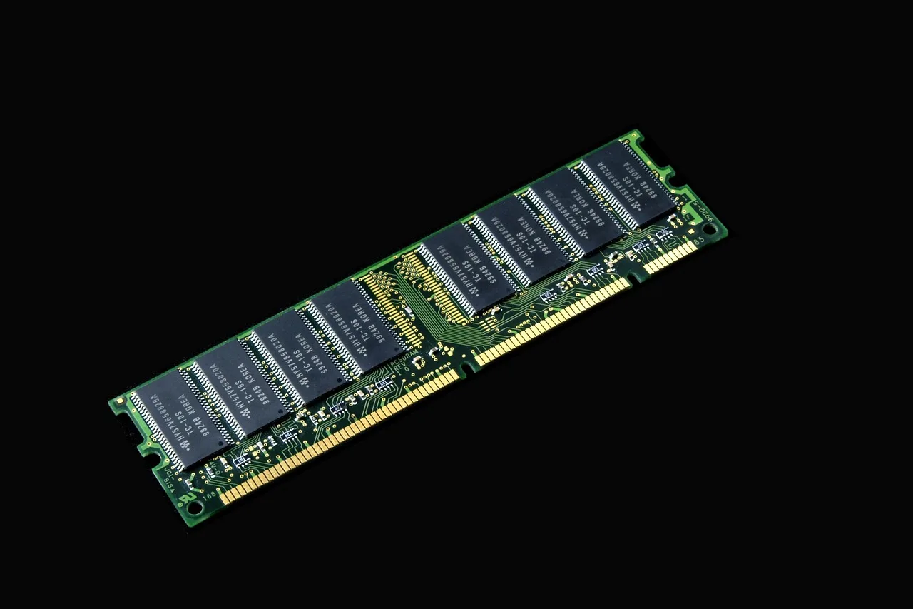
SK Hynix is advancing its chip inspection technology, because 3D memory structures are pushing conventional metrology to its limits, Digitimes reports.
That's the whole story in one line, but the implications run wide. Metrology — the science of measuring chip features during manufacturing — determines whether a wafer ships or gets scrapped. Get it wrong at 3D scale, and yields collapse.
Why does 3D memory break inspection?
Conventional metrology tools were built for chips whose critical structures sit largely in one plane. 3D NAND and high-bandwidth memory (HBM) stack cells vertically in dozens of layers, which buries defects deep inside the stack where optical and conventional inspection methods struggle to see them.
A defect on layer 80 of a tall stack is invisible from the top. Traditional top-down inspection can't reach it. That's the physics problem SK Hynix is working against.
What is SK Hynix actually doing?
The company is advancing its inspection capabilities to close that gap, according to the report. Specific tool types, partners and timelines weren't disclosed in the source material, so we won't speculate here. What's clear is the direction: better defect detection inside vertically stacked structures.
The move matters because inspection quality feeds directly into yield — the share of usable dies per wafer. In stacked memory, one undetected defect can kill an entire tower of cells, not just a single layer.
What does this change for the memory market?
For buyers, better inspection means higher yields on high-layer-count NAND and HBM, the memory used in AI accelerators. Higher yields typically mean more supply at lower cost per bit.
For competitors — Samsung and Micron face the same physics — SK Hynix's progress sets a pace. Every memory maker stacking higher needs metrology that keeps up.
For tool vendors, it's a signal. Memory makers hitting metrology walls tend to co-develop new inspection approaches with equipment suppliers, and that spending flows into the semiconductor capital-equipment market.
We'll track specifics — tools, vendors, yield figures — as they surface.
via Google News: DRAM chip (Source)
More from Grace Kim
Show full bio
Market editor covering regulation, policy and their impact on hardware layer of artificial intelligence at Die Signal.
470 articles
Same lot · LOT-C1E5
- DSG-68705nmSK hynix names Onto Innovation Best Partner for HBM defect control
- DSG-724028nmSK hynix hands Onto Innovation partner award for HBM defect detection
- DSG-876928nmSK hynix Names Onto Innovation Best Partner for HBM Defect Prevention
- DSG-263065nmSK hynix honours Onto Innovation for HBM defect detection work
- DSG-320828nmOnto Innovation Takes SK hynix Best Partner Award for HBM Defect Work