Test report DSG-6183 · Rev D · tested October 30, 2026
Foundries & ManufacturingDevice under test
China Builds 5nm-Class Chips Without EUV, But the Cost Curve Steepens
SMIC is nearing 5nm-class density with DUV multiple patterning, but four 193nm masks already cost more than one EUV exposure. Experts see a hard economic limit.
- Read
- 4 min
- Words
- 849
- Node
- 3nm
- Operator
- Marcus Bennett
Spec summary
- Teardowns in 2023 showed SMIC built Huawei's Kirin 9000S on a 7nm-class process without EUV; the Kirin 9030 approaches 5nm-class density.
- Three exposures on a 193nm tool cost about the same as one EUV exposure; at four masks EUV becomes cheaper, Chris Mack said.
- Morgan Stanley estimated CXMT produces about one-third as many bits per wafer as Western DRAM makers.
- Micron's 1-gamma DRAM with EUV achieves over 30% higher bit density per wafer than 1-beta.
- Morgan Stanley projects China's AI chip self-sufficiency rising from 42% in 2025 to 70% by 2030.
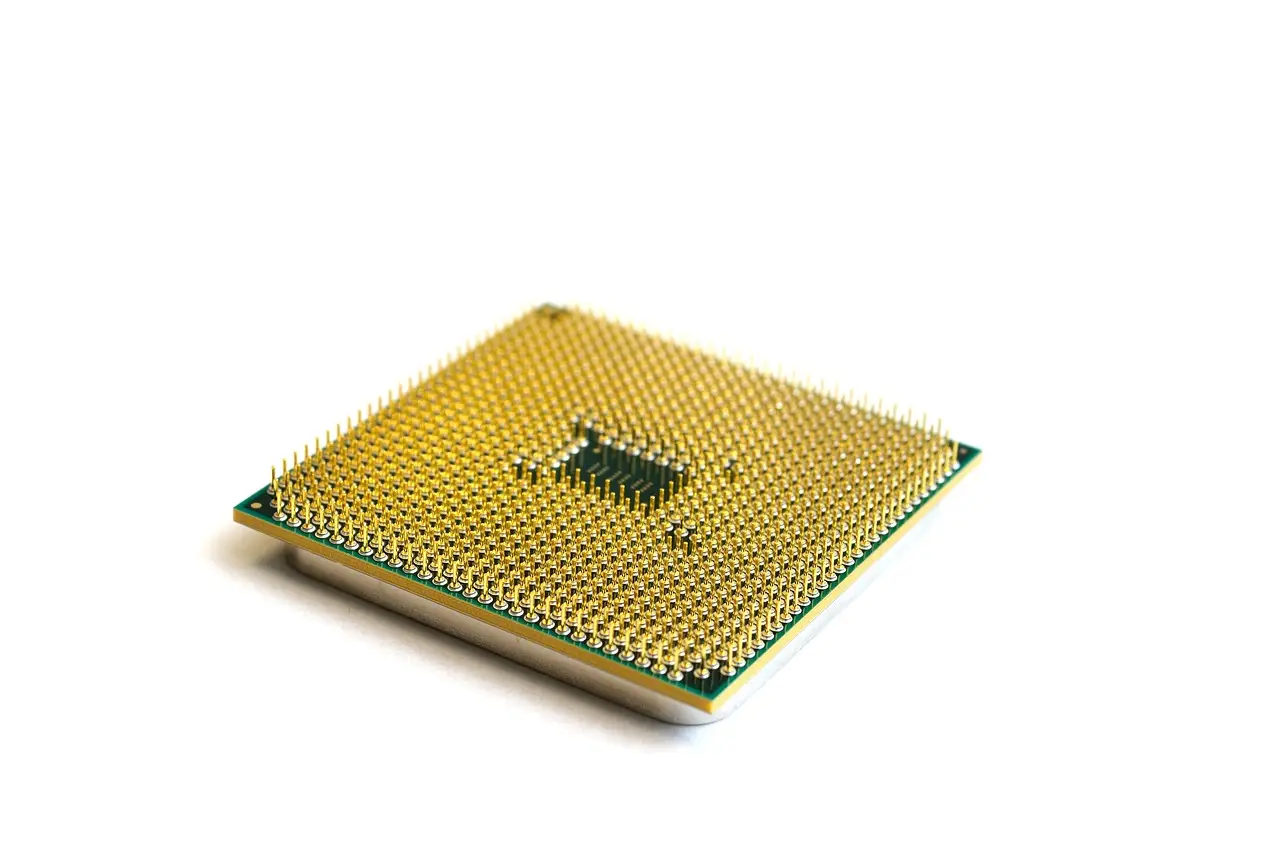
China's SMIC has pushed DUV-based manufacturing close to 5nm-class density without a single EUV machine, but experts say the economics of multiple patterning grow worse with every added exposure. Lithography expert Chris Mack puts the crossing point at three masks.
"At three, it was about even," Mack, co-founder and CTO of Fractilia, said in an interview. "But as soon as you hit four masks – 193 masks being replaced by one EUV mask – then EUV became more cost-effective."
Export controls keep ASML's extreme ultraviolet systems, which use 13.5nm-wavelength light, out of China. The EUV gap between China and the West is at least half a decade, according to some analysts. Chinese manufacturers have answered with older deep ultraviolet tools and repeated exposures.
Teardowns of Huawei's Mate 60 Pro in 2023 found the Kirin 9000S processor made by SMIC on a second-generation 7nm-class process. More recent analysis of the Kirin 9030 shows SMIC approaching the density of 5nm, though still behind TSMC and Samsung. Reporting on SMIC's N+3 process suggests progress toward 5nm, but measured scaling remains significantly behind established 5nm processes.
How does multiple patterning work?
The method splits one intricate chip layer into several simpler patterns. The wafer passes through the lithography tool repeatedly, and each pass etches part of the final design.
Each exposure must line up perfectly with everything already etched beneath it. More exposures mean more overlay errors and accumulating process variation. "If you have, say, four 193 masks, you've got all those different overlays, and you've got all these different process variations that start to accumulate," Mack said.
Designers can leave more space around features to make manufacturing reliable. That makes the die bigger. Fewer dies fit on a wafer, and wafers cost tens of thousands of dollars each.
"You don't sell wafers, you sell die," Mack said. "The question is: how many die can I fit onto that wafer, and how many of those die yield, and therefore how many chips can I sell per wafer?"
What does the efficiency gap look like in practice?
Morgan Stanley estimated in a June report that Chinese DRAM maker CXMT produces roughly one-third as many bits per wafer as Western competitors. The analysts attributed about a third of that shortfall to the older process node and called lithography access a "hard ceiling" on Chinese memory development.
Douglas Fuller, a researcher at Copenhagen Business School, said: "For advanced logic chips, in theory there could be other innovations to engineer around EUV, but they are not likely to be very efficient and effective."
Mack also cautioned against node labels: "If somebody says it's X node – the seven nanometer node, the five nanometer node, the three nanometer node – these words almost have no meaning."
How far can DUV stretch?
Micron shows the ceiling is high. Its 1-alpha DRAM generation was developed without EUV using 193nm immersion lithography and multiple patterning.
"They pushed 193 farther than any of the other memory makers did," Mack said. "They were able to make very competitive chips with 100% 193 compared to Samsung and Hynix making them with many layers of EUV."
Morgan Stanley believes CXMT's planned move to 1-alpha DRAM, intended for HBM3e, is achievable without EUV, citing Micron as evidence. Fuller reckons that "by the end of the decade, advanced packaging will allow firms to use DUV to produce the latest generations of DRAM."
Micron also designed products around its available tools rather than copying EUV processes. Mack said China "could probably push a long way with 193 multiple patterning" if the full 193nm ecosystem were available and designs were optimized for it.
Memory's repetitive structures make that coordination easier than for logic chips. "Memory is a lot easier than logic," Mack said. Micron itself switched: its 1-gamma DRAM process uses EUV and delivers more than 30% greater bit density per wafer than the preceding 1-beta generation.
EUV is not a magic wand either. Stochastic effects — random variations from the small number of photons in an exposure — force manufacturers to raise the dose, which pushes cost back up.
What does this change for China's chip plans?
Mack sees an economic limit. "I would be hard pressed to really believe that a three nanometer or a two nanometer node is going to be economically viable without EUV," he said.
Chinese chipmakers will not hit a wall and stop. They can accept larger dies, lower yields, longer manufacturing times, or all three. Morgan Stanley assumes CXMT stays on 1-alpha without EUV yet still grows its share of global DRAM bit supply from 14% in 2026 to 16% in 2028 through greenfield capacity. The bank also expects China's AI chip self-sufficiency to rise from 42% in 2025 to 70% by 2030, aided by new capacity, improving yields and heavy state support — while EUV, HBM and advanced software leave a persistent gap.
Without EUV, the experts conclude, China can only get partway to bridging the gap with the West.
via Tom's Hardware (Source)
More from Marcus Bennett
Show full bio
News editor covering regulation, policy and their impact on hardware layer of artificial intelligence at Die Signal.
524 articles
Same lot · LOT-C204
- DSG-839645nmChinese Semiconductor Tool Vendors Gain Share Under U.S. Sanctions
- DSG-117945nmASML Shares Fall on China Restrictions Despite Strong Results
- DSG-923010nmChina amasses hundreds of ASML DUV scanners for 7nm AI output
- DSG-96303nmChina Stockpiles 343 Immersion DUV Systems, Targeting 7-nm AI Base
- DSG-356110nmNaura Says Breakthrough Could Let CXMT Build 3D DRAM Past EUV Ban